




A new silicon carbide transistor architecture improves high-temperature control and leakage performance, enabling reliable electronics for extreme environments where conventional semiconductor devices struggle.
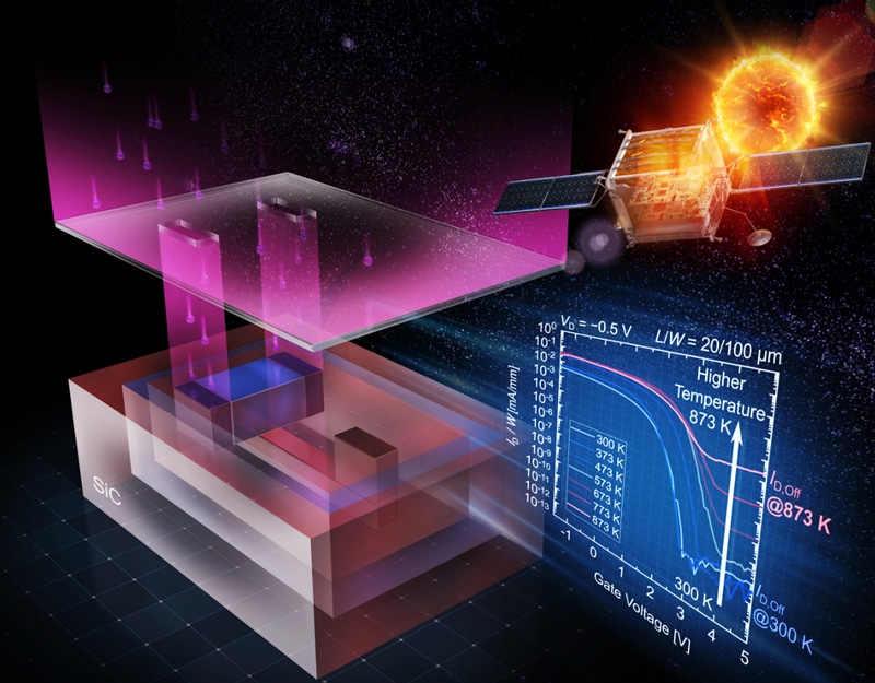
A new silicon carbide (SiC) junction field-effect transistor (JFET) has demonstrated stable operation at 600°C, addressing two major barriers that have limited the use of SiC for extreme-temperature integrated electronics: poor threshold-voltage control and excessive leakage current. Researchers at Kyoto University developed the device using a redesigned transistor architecture that exploits SiC’s intrinsic material properties.
The key change is a bottom-gate structure rather than the conventional top-gate configuration used in earlier SiC JFETs. This architecture gives engineers better control over the transistor’s threshold voltage, allowing the device to switch more predictably as temperature rises. The researchers also replaced the semi-insulating SiC substrate traditionally used for these devices with well-based isolation. This helps electrically isolate device regions while suppressing leakage currents that become increasingly problematic at elevated temperatures.
High-temperature operation is particularly demanding for semiconductor devices because rising temperatures can increase unwanted current flow and alter electrical characteristics. Previous SiC JFET implementations showed both limited controllability and substantial leakage under such conditions. The new architecture tackles these limitations simultaneously, bringing measured leakage close to the theoretical level expected from SiC’s material properties.
The researchers fabricated the transistor using industry-standard manufacturing approaches, rather than developing an entirely new fabrication process. This is significant for eventual scalability because the structure is intended to build on established semiconductor manufacturing techniques.
The demonstrated 600°C operation points toward electronics capable of functioning in environments that exceed the practical temperature range of conventional silicon devices. Potential areas include monitoring and control electronics positioned close to high-temperature machinery, industrial systems, and other extreme-environment applications.
The work also supports the development of complementary SiC JFET circuits, which could enable low-power integrated circuits designed for extreme temperatures. However, the technology remains at an early development stage. The next steps include building more complex circuits, moving toward wafer-level fabrication, and developing packaging capable of maintaining reliability under extreme thermal conditions.


