


A new lamination approach enables stable, uniform production of large-area flexible electronics, improving yield, adhesion control, and scalability for next-generation displays, sensors, and advanced semiconductor packaging systems.
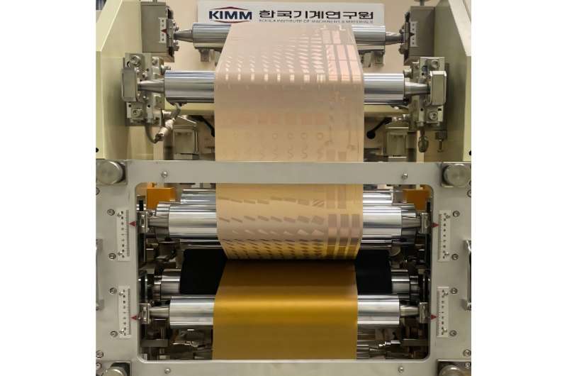
A research team at the Korea Institute of Machinery and Materials (KIMM) has developed a roll-to-roll direct lamination process that enables continuous packaging of long-length flexible printed circuit boards (FPCBs), addressing key scalability and process-stability challenges in large-area electronics manufacturing.

The approach replaces conventional batch lamination with a continuous manufacturing flow, improving process stability and scalability. By maintaining consistent pressure, temperature, and adhesive flow across long substrates, the method reduces variations that typically lead to delamination, void formation, and structural stress in large-format circuits.
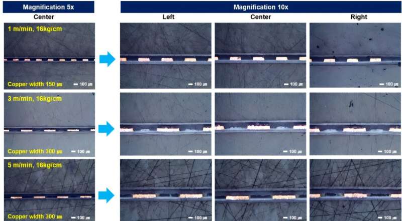
A key strength of the technique is its enhanced control over adhesive behaviour under varying process conditions. Through detailed analysis of bonding material flow and optimisation of lamination parameters, the researchers achieved more uniform interface contact, improving both electrical reliability and mechanical durability of FPCBs.
The development comes as demand for large-area electronics rises across automotive, consumer electronics, and industrial applications. Electric vehicles, in particular, are driving the adoption of lightweight, flexible interconnects to replace traditional wire harness systems. The process also supports integration with data-driven monitoring and AI-assisted manufacturing, enabling more adaptive and efficient production environments.
Industry experts view continuous lamination as part of a broader transformation in electronics manufacturing, where yield improvement, defect control, and scalability are becoming as critical as material innovation. Similar advancements are also being explored in advanced packaging and substrate technologies for AI and high-performance computing applications.
The method is expected to improve production yields while reducing manufacturing costs in high-volume environments, especially as demand grows for flexible and large-format electronic designs. Stable lamination processes are likely to play a foundational role in next-generation electronics production ecosystems.
Dr. Jun Sae Han said, “This study demonstrates the feasibility of packaging long-length FPCBs using a continuous process.” He added that the team plans to expand its applications across various electronic devices and develop it further into intelligent and autonomous manufacturing systems through integration of real-time process monitoring and non-destructive inspection techniques.
The research marks a step forward in flexible electronics manufacturing, tackling long-standing challenges in maintaining uniform adhesion and structural integrity across extended production lengths while enabling industrial-scale deployment.
