
By slashing power loss with world-first soft switching and offering ramped and stepped waveforms, the innovation promises sharper etching, longer device life, and scalability beyond semiconductors into defense, healthcare, and environmental applications.
For advanced chipmaking, researchers at Korea Electrotechnology Research Institute (KERI) have unveiled a tailored pulsed power modulator for bias—a technology that promises unprecedented precision in semiconductor fabrication. Bias power is central to plasma-based processes such as etching, cleaning, and thin-film deposition. Conventional radio-frequency (RF) supplies, while industry standard, rely on simple alternating waveforms that fall short of the ultra-fine control needed for semiconductor geometries.
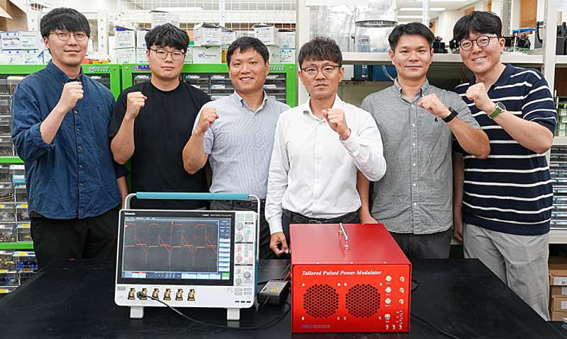
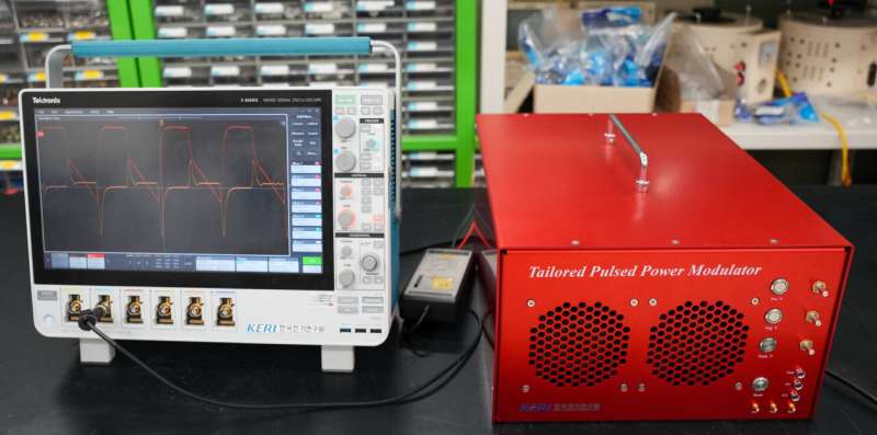
The team, led by Dr. Jang Sung-roc, has engineered a pulsed system capable of generating customized bias forces at extreme speed and voltage. Unlike traditional RF sources, this modulator stores energy over time and releases it in powerful, finely tuned bursts. The result: wafer etching with sharper, deeper, and more uniform profiles.
The challenge, however, lies in managing energy loss during instantaneous discharges reaching several kilovolts at frequencies up to 400 kHz. Conventional pulsed supplies typically waste power and generate excessive heat. To overcome this, the team became the first in the world to apply soft switching to semiconductor bias supplies. By switching precisely when voltage or current approaches zero, they cut power loss by over 78%, reduce heat stress, and extend device lifespan—all while enabling smaller, denser power systems.
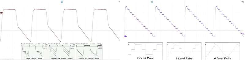
The researchers designed the system with two modes: ramped waveforms for compact, precise processing, and stepped waveforms that create diverse patterns needed for different fabrication tasks. This flexibility makes the technology adaptable not only for semiconductors but also for defense, healthcare, and environmental systems where pulsed power is critical.
Validation inside a semiconductor process chamber—through collaboration with the Korea Institute of Fusion Energy—confirmed the ability to generate unique, controllable waveforms. KERI now plans to apply the modulator in real etching and cleaning equipment in partnership with the Korea Institute of Machinery & Materials.
With patents secured, the institute is preparing for commercialization through joint industry and research efforts. As Dr. Jang notes, tailored pulsed power could be the catalyst for “smaller, faster, and longer-lasting electronic devices,” addressing the bottlenecks faced by manufacturers seeking next-generation process solutions.