
New MIT process embeds matching hardware fingerprints in paired chips for direct, server-free authentication.
Researchers at the Massachusetts Institute of Technology have unveiled a novel chip-fabrication technique that could reshape hardware-level security for electronic systems by enabling paired microchips to authenticate one another directly using shared physical identifiers.

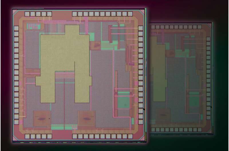
At the core of the approach is the creation of paired physical unclonable functions (PUFs)—hardware fingerprints arising from microscopic manufacturing variations inherent to CMOS (complementary metal-oxide-semiconductor) chips. Traditional PUF-based authentication methods rely on storing secret reference responses on external servers, a practice that introduces potential vulnerabilities and added overhead in memory and computation. The new method sidesteps that requirement by instilling identical fingerprints into two chips during fabrication.
The technique works by designing two adjacent dies on a silicon wafer with linked transistor structures along their shared edge. Researchers induce controlled gate oxide breakdown in paired transistors using low-cost LEDs. Because each transistor’s breakdown timing is influenced by random microscopic variations, the resulting state serves as a unique fingerprint. By structuring transistor pairs across two chips before the wafer is diced, each resulting device ends up with a highly correlated PUF. Prototypes have achieved over 98 % reliability in matching these twin fingerprints.
Once separated, the paired chips can verify each other’s identity directly without communicating with a third-party server or storing secret keys off-chip—addressing a key pain point in existing cryptographic device authentication. This could benefit energy-constrained electronics such as medical sensors and wearable systems, where minimizing protocol overhead and external dependencies is critical. For instance, an ingestible sensor and its paired wearable patch might authenticate securely and efficiently with this method.
Importantly, the process is compatible with standard CMOS foundry fabrication and does not require exotic materials or complex post-processing, potentially easing adoption in commercial semiconductor production. Researchers suggest future iterations could preserve the shared randomness deeper within transistor structures to further strengthen hardware security at the physical level.
The development marks a step toward embedding cryptographic trust directly in silicon, reducing reliance on external key storage and simplifying secure authentication for next-generation electronics.