


A new film-thickness measurement system promises to collapse wafer inspection times delivering full 300 mm-wafer thickness maps in under a heartbeat and boosting throughput for semiconductor fabs.
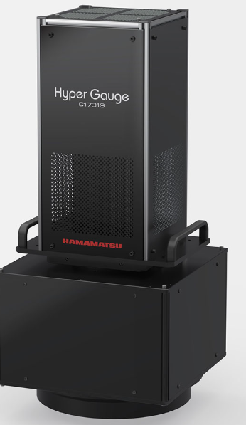
The latest entrant to wafer metrology is a thickness measurement device from Hamamatsu Photonics that promises to transform semiconductor process control. The new system delivers full-surface thickness distribution for 300 mm wafers in just 5 seconds, a dramatic speed-up compared with traditional point-by-point measurement methods.

The key features are:
- Measures film-thickness distribution across a full 300 mm wafer in just 5 seconds
- Utilizes proprietary “λ-Capture” wavelength detection via high-sensitivity camera no spectrometer needed
- Offers high spatial resolution and repeatability, suitable for both bare and patterned wafers.
- Covers thickness range from ~10 nm up to ~1000 nm with precision (e.g., ±1 nm for thin films)
- Maps thickness over ~750,000 points per wafer in a single pass enabling complete in-plane distribution analysis, rather than sampling
Behind the acceleration is a proprietary wavelength-detection method that eschews bulky, slow spectrometers in favor of a high-sensitivity camera, enabling area-based thickness mapping across hundreds of thousands of points in a single snapshot. Because the entire wafer is imaged at once, there’s no need for time-consuming alignment or repeated scanning translating directly into faster cycle times and reduced process losses.
Beyond speed, the meter offers high spatial resolution and strong measurement reproducibility whether inspecting bare wafers or patterned ones. That makes it suitable not only for conventional film-thickness checks, but also for monitoring uniformity across complex, patterned wafers that are routine in modern semiconductor fabrication. With its fast full-surface coverage, the tool fits neatly into inline inspection workflows, helping fabs catch thickness variation issues early, a critical factor for yield and quality assurance as process geometries shrink.
This kind of high-speed, high-coverage thickness measurement could be a boon for modern fabs, especially those dealing with complex thin films or tight uniformity specs.