


Ultra thin electronic layers may fail due to atomic faults. A new method reveals these weak spots before devices break down.
Researchers in the United States have developed a way to detect hidden defects in ultra-thin electronic materials that can cause devices to fail at lower voltages. A team at Rice University showed that tiny defects in hexagonal boron nitride, a common two-dimensional insulator, can trap electrical charges and weaken specific regions of the material. These weak spots allow current to leak earlier than expected, which can lead to device failure. Two devices made using the same process may behave differently if one contains these hidden fault lines.

The study examined layered electronic structures known as heterostructures. These are built by stacking different two-dimensional materials. Hexagonal boron nitride is often used in these stacks because it provides a flat and stable insulating layer between active materials.
The researchers found long, narrow misalignments in the atomic layers of hexagonal boron nitride. These defects, called stacking faults, resemble slight shifts between pages in a book. Although they can form easily, they are difficult to detect with standard inspection tools.
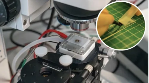
To understand how the faults form, the team peeled thin flakes from a bulk crystal using adhesive tape and transferred them onto silicon and silicon dioxide wafers. They suspected that bending during this transfer process could introduce stacking faults.
The same flakes were examined before and after transfer. Optical and atomic force microscopes showed smooth surfaces. However, when the samples were analyzed using cathodoluminescence spectroscopy, which scans the material with an electron beam and records emitted light, bright and narrow fault lines become visible.
The results showed that thicker flakes were more likely to develop these faults. In regions with stacking faults, the material’s insulating performance dropped, and electrical leakage started at lower voltages.
By combining electron microscopy, cathodoluminescence mapping and force-based measurements, the team created a practical method to identify these hidden defects before devices are put into operation. The approach can also be applied to other layered materials used in ultra-thin electronics.
