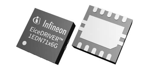
Minimized R&D efforts and costs as well as robust and highly efficient operation of medium-voltage gallium-nitride (GaN) switches are key requirements for modern power electronics systems. In accordance with its strategically-designed GaN product portfolio to continuously strengthen full system solutions, Infineon Technologies AG introduces the EiceDRIVER 1EDN71x6G HS 200V single-channel gate driver ICs family. The new product family is designed to enhance the performance of CoolGaN Schottky Gate (SG) HEMTs but is also compatible with other GaN HEMTs and Silicon MOSFETs. The gate drivers aim at a wide range of applications including DC-DC converters, motor drives, telecom, server, robots, drones, power tools, and class D audio amplifiers.

1EDN71x6G variants come with selectable pull-up and pull-down driving strengths, enabling waveform and switching speed optimization without the need for gate resistors. This leads to a smaller power stage layout with fewer BOM components. The strongest/fastest driving variant (1EDN7116G) is suitable for half-bridge configurations with significant paralleling. The weakest/slowest driving variant (1EDN7146G) can be employed for some dv/dt-limited applications like motor drives or very small-die GaN (high-RDS(on), low Qg) HEMTs. Each variant also has a different blanking time, proportional to the minimum recommended dead-time, the minimum pulse width, and the propagation delay.
The truly differential logic input (TDI) feature eliminates the risk of false triggering due to ground bounce in low-side applications and enables 1EDN71x6G to address even high-side applications. Additionally, all variants feature an active Miller clamp with an exceptionally strong pull-down to avoid induced turn-on. This offers extra robustness against glitching in the gate driving loop, especially when driving transistors with a high Miller ratio.
Furthermore, 1EDN71x6G offers active bootstrap clamping to avoid overcharging the bootstrap capacitor during dead-time. This provides bootstrap supply voltage regulation that protects the high-side transistor’s gate without requiring an additional regulation circuit. An optional programmable charge pump with adjustable negative turn-off supply is also provided for additional Miller-induced turn-on immunity when needed, e.g. when PCB layout cannot be fully optimised.


