In the previous part of this article we started learning about the trends and challenges of 7nm IC technology. Let us learn more about the same.
How EUV is different from older lithography technologies
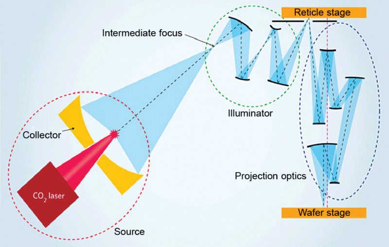
There are multiple ways that extreme ultraviolet (EUV) differs, mostly associated with the methods to create and transport the short-wavelength light. Traditional lenses cannot be used with EUV as these absorb light. A mirror with a highly-specialised coating, called a multilayer mirror, must be used. Even these special mirrors absorb about 30 per cent of light, so it is advantageous to use as few as possible. Any gas in the light path, such as air or nitrogen, will also absorb the light, thus, the entire light path is inside a vacuum chamber.

While source power is the chief concern due to its impact on productivity, significant changes in EUV mask infrastructure, including blanks, pellicles and inspection, are also under study. Particle contamination would be prohibitive if pellicles were not stable above 200W, the targeted power for manufacturing. Without pellicles, particle adders would reduce yield, which has not been an issue for conventional optical lithography with 193nm light and pellicles.
Current lack of any suitable pellicle material, aggravated by the use of hydrogen plasma cleaning in EUV scanner, is preventing the adoption of EUV lithography for volume production. Some issues not specific to EUV such as resist collapse and stochastic effects (including photon shot noise) also currently bar EUV from exceeding resolution limits of immersion lithography in high-volume manufacturing.
Double patterning is expected for EUV for random logic patterns at 7nm node (32nm pitch) due to the need for dipole illumination. 5nm node (22nm pitch) would likewise be expected to use multiple patterning already being developed for immersion lithography. However, IBM must hope it can reduce the cost by the time 7nm chips are ready to be manufactured in a few years.

IBM is expected to go beyond 7nm by the end of the decade, but it also recognises that it will be a much harder task. Scaling to 7nm and below is a terrific challenge, calling for deep physics competencies in processing nano materials affinities and characteristics. New materials such as carbon nanotubes or graphene will be necessary to go beyond 7nm. The alternative could be to start developing other types of computers such as quantum, cognitive or neuromorphic.
Currently, state-of-the-art lithography has a wavelength that is 193nm wide, which makes it quite difficult to design chips with much smaller transistors. EUV lithography, on the other hand, has a wavelength of only 13.5nm. EUV lithography is still much more expensive to use because it must operate for longer periods of time and is sensitive to the smallest vibrations when designing chips.
Self-aligned quadruple patterning
As 193nm immersion lithography is reaching its optical resolution limit using single exposure, advanced multi-patterning concepts are being studied to reach lower nodes. Targeting the node, self-aligned quadruple patterning (SAQP) is an advanced patterning approach that uses pitch splitting to extend the capability of double-patterning 193nm immersion lithography. Using parallel interpretation of multiple scatterometry targets with slightly variable pitches, researchers have revealed that scatterometry is capable of measuring different space populations, and developed metrology solutions can be utilised to monitor and control each process step of SAQP patterning.
Next-generation transistor is called nanowire FET, which is FinFET turned on its side with a gate wrapped around it. Nanowire FET, sometimes called a gate-all-around FET, is said to meet the device requirements for 5nm, as defined by International Technology Roadmap for Semiconductors. It has paved the idea of making switch-in-transistor architectures down the road and is developing technologies in the arena.
Chipmakers see a path to extend today’s FinFETs to 7nm, but 5nm is far from certain and it may never happen. Indeed, there are a multitude of technical challenges at 5nm. And the cost for 5nm is expected to be astronomical. Performance and cost concerns are the big challenges in scaling to 5nm, and addressing these will involve extension of current approaches as well as introduction of new technologies and materials. If the industry moves forward with 5nm, and so to help the industry get ahead of the curve, semiconductor engineering has assembled a list of some of the more challenging process steps at 5nm.
Patterning and mask making
For 7nm and beyond, patterning is the biggest challenge. This technology has to be production worthy, with the right uptime of tools and an economic throughput per day. In theory, EUV simplifies the patterning process. With 193nm immersion and multiple patterning, there are 34 lithography steps and 60 metrology steps at 7nm. This compares to just six lithography steps and seven metrology steps for 28nm. With EUV, there are just nine lithography steps and 12 metrology steps at 7nm. Even so, chipmakers still require both EUV and multiple-patterning at 7nm and beyond. And ultimately, the decision to put EUV into production depends on the maturity of the power source, mask infrastructure and resists.Today, oft-delayed EUV source can generate 80 watts of power. But chipmakers want 250 watts to bring EUV into mass production. It has to show reliability and availability. There are other issues as well. As lines become narrower at each node, the industry faces a growing and problematic issue called line-edge roughness. Basically, line-edge roughness is a deviation on the edge of a line. It is a line-width variation that does not scale with feature size. Meanwhile, as before, lithography is tied to the photomask.
At 7nm, photomask makers may need to prepare for both traditional optical and EUV masks. Optical masks are complex and expensive at 7nm. Because of the increased demand on the process window for the wafer, shapes drawn on masks are becoming smaller. EUV mask shapes are less complex than ArFi (193nm ArF immersion) at those nodes.
But EUV brings other issues on the mask. For example, correction for shadowing and other effects at wafer level has the potential to explode mask data volumes.
Another example is mid-range correction that becomes necessary for EUV masks because of wider dispersion of electrons during the mask-making process as these hit the multi-layer reflective mask.
Fab flow and variation
Patterning, CMP, deposition, etch and other process steps are challenging at 7nm and 5nm. Future devices would require structures with thin, precise and conformal films. And chipmakers would continue to grapple with structures that consist of only a finite number of atoms. It almost seems like a lot of technologies are all being worked on in parallel.
Manufacturing with yield and having reliable devices would be difficult to do.
With those factors in mind, chipmakers face a sometimes-overlooked challenge, namely, process variation. Variation can be defined as any deviation from intended goal. There are various sources of variation in the fab, including within the die, within the wafer and between one tool chamber and another chamber. Variation control is really dropping down to atomic scale. Gate’s critical dimension uniformity requirements are in angstroms not nanometers.
Selective processes
At current and future nodes, chipmakers would require newfangled technologies called selective deposition and selective removal. Combining novel chemistries with atomic-layer deposition or molecular-layer deposition tools, selective deposition involves a process of depositing materials and films in exact places.
Basically, most of our processing today is done based on line-of-sight capability. But soon, these would begin to tunnel through structures and build structures that you cannot see through from the top. So the industry needs to find a way to do selective deposition. Those techniques are somewhat there, but are not mature enough.
Chipmakers, R&D organisations and universities are all working on selective deposition. Materials must also be removed using a related technology called selective removal or atomic-layer etch. This is a next-generation plasma etch technology that enables layer-by-layer, or atom-by-atom, etching. Atomic layer processing is the norm now for many applications.
Interconnects
In chip production, back-end-of-line is where interconnects are formed within a device. Interconnects and tiny wiring schemes in devices are becoming more compact at each node, thereby causing a resistance-capacitance delay in chips. Back-end-of-line would require new tools and materials. But if you make it taller, you may have more resistance-capacitance.
At 5nm, problems become worse. These occur due to the way wiring is done in the interconnect. It is not just in resistance and capacitance, but in how to wire up the transistor. We are seeing a lot of congestion. For that reason, the industry may need to consider an alternative path. This argument pushes us into doing 3D stacking.
Inspection and metrology
Optical inspection, the workhorse technology in the fab, is struggling to detect defects at 20nm and below. e-beam inspection can find tiny defects, but the technology is slow. Optical inspection tools operate at wavelengths down to 190nm. Seeking to capture more defects, a sub-190nm wavelength technology is used.
In addition, the industry is working on next-generation technology called multi-beam e-beam inspection. But this technology might not be ready until 2020. Exact timing will depend on how quickly the core technology can be scaled in terms of the number of beams and beam current.
Meanwhile, metrology, the science of measuring structures and films, is another concern. Today’s metrology tools are capable of measuring structures in two dimensions, and in three dimensions to some degree. But that is not nearly enough for the complexity of current and future devices. In fact, there is no single metrology system that can measure everything. So chipmakers must use several different metrology tools in the flow.
As the industry moves to 7nm and 5nm, there will be a drastic decline in signal-to-noise ratio of metrology tools. To compensate this uncertainty of measurements from each tool, there would be an even greater need for a multiple metrology approach. This means hybrid metrology is inevitable. In hybrid metrology, chipmakers use a mix and match of several different tool technologies and then combine data from each. Hybrid metrology, however, is still in developing stage. Fortunately, this silicon alternative does not have any major physical flaw like most other materials.
Silicene and germanene, for example, degrade within a few minutes or hours, while graphene is not suitable for all transistor types and is still extremely challenging to use in the production of integrated circuits due to fragility of its structure. InGaAs and InP based devices can be manufactured using existing techniques in combination with silicon.
The main issue remains to be yield and cost. Beyond 14nm, as we move to 10nm and 7nm, a new fin material will be required—probably silicon-germanium (SiGe), or perhaps just pure germanium. SiGe and Ge have higher electron mobility than Si, allowing for lower voltages and, thus, reducing power consumption, tunneling and leakage.
SiGe has been used in commercial CMOS fabrication since the late 1980s, too, so switching from silicon would not be too painful. The primary reason that we have been using silicon for so long is that the entire industry is based on silicon. The amount of time, money and R&D that would be required to deploy new machines for handling new materials that we know relatively little about would be astronomical.
SiGe would take us to 7nm, but after that we are probably looking at a new transistor structure. Just as FinFET created a larger surface area, mitigating the effects of quantum tunneling, both gate-all-around FETs and vertical tunneling FETs would again allow for shorter gates and lower voltages.
Gate-all-around FET essentially consists of nanowire source and drains, surrounded by a gate. A vertical tunneling FET is similar in a way that it uses nanowires, but the actual method of operation is very different from conventional FETs. TFETs allow for lower operating voltage.
Another option is a somewhat conventional FinFET, but with fin constructed out of III-V semiconductors such as gallium-arsenide (GaAs), which again have higher electron mobility than silicon. There may be better gains to be had from moving sideways, to materials and architectures that can operate at faster frequencies and with more parallelism, rather than brute-forcing the continuation of Moore’s law.
Meaning, the pitch or distance between major features on the chip are still scaling at an expected rate. Reduction in distance between fins, the raised channels behind the name FinFETs, is right on target (0.70x), the distance between gates on top fell just short (0.78x), but the interconnects scaled further than expected (0.65x), thanks in part to the introduction of a new feature, airgaps, that reduces cross-talk between interconnects spaced so closely together. The result is that overall logic area scaling continues.
IP reuse and foundry business
All semiconductor companies develop intellectual property (IP) that they use in their own products or licence to others. For example, 3G and 4G technologies are not just for smartphones and tablets. Development of IP also helps semfab with development partners and with its growing foundry business.
Today, these customers are bringing their own designs using their IP, supplemented with technology, but eventually plan to offer their own IP to customers. As semiconductor manufacturing grows more difficult and expensive, and the number of players dwindles (from 18 a decade ago to just four today in advanced logic), manufacturing edge grows more compelling to other companies.
Enterprise IT hardware is still big and important, but other customers include Cloud service providers, telcos and technical computing. Growth drivers are Cloud architectures, software-defined networks and network-functions virtualisation for communications, high-performance computing and, of course, Big Data and analytics.
And it is getting an increasing share of its revenues from other data centre technologies including storage controllers and Ethernet switches, silicon photonics to replace fibre and copper, fabrics and switches and communications gear. The Internet of Things (IoT), software and services and memory sometimes get lost in the shuffle, but each is on track for more than US$ 2 billion in sales this year.
Although gadgets like MICA bracelet, Basis Peak smartwatch and SMS audio smart earbuds get lots of press, the IoT business is growing quickly due to applications such as retail, automotive and manufacturing.
The software business is growing more strategic and Intel has said, it believes that mobile devices based on its silicon will be the first—other than Nexus-branded ones—to get Android 5.0 Lollipop update.
The memory business, a joint venture with Micron, is shifting from selling memory chips to developing clients and enterprise SSDs, which are increasingly important to close the widening performance gap between CPUs and hard drive based storage.
Transistor options
You must select the right transistor architecture for 5nm. Today, there are two leading options: finFET and nanowire FET. Scaling FinFET to 5nm is challenging. In a 5nm FinFET, for example, fin width is projected to be 5nm, which is supposedly the theoretical limit for this structure. That is why chipmakers are exploring nanowire FET.
Nanowires have good electrostatics. But these come with other issues such as device width of nanowires and how much current you can get out of devices. Those are the areas that people are flushing out.
Mask making
In process flow, meanwhile, photomask manufacturing is one of the first steps. As before, lithography determines mask type and specs. So if 5nm happens, the photomask industry will likely need to develop masks for two lithography types—optical and EUV lithography. Making an optical mask will be daunting at 5nm. Bringing up EUV mask line is also difficult, as these are very different from 193i masks in many ways.
Because it is such a massive change, it will have a huge impact on features or capabilities of every product in the supply chain. This includes resists, masks and pellicles, as well as equipment like e-beam writers and even software.
On EUV mask front, the industry is making progress in some areas, but not in others. Mask blank inspection is a bright spot. EUV mask inspection and pellicles are question marks. For 5nm, though, mask write times will be the biggest challenge. Today’s single-beam e-beam tools are unable to pattern complex masks fast enough and in a cost-effective manner.
There is a solution. Two groups, IMS/JEOL duo and NuFlare, are separately working on a new class of multi-beam e-beam mask writers. The tools, which promise to accelerate write times, are expected to ship soon. Reports have surfaced, however, that development of these tools is taking longer than expected due to technical issues. Any disruptive new technology like this will take time to mature before it reaches high-volume production.
Patterning
After the mask is made, it is shipped to the fab. The mask is placed in a lithography tool. Then, the tool projects light through the mask, which, in turn, patterns images on a wafer. Needless to say, patterning is one of the big question marks at 5nm. For this, chipmakers hope that EUV is finally ready for 7nm and 5nm. This, of course, depends on the status of the power source, resists and mask infrastructure.
In theory, EUV will simplify the patterning process, thereby reducing cost. But even if EUV happens at 7nm and/or 5nm, chipmakers would require a form of multiple patterning.
Here is a worse-case scenario. If EUV misses the window at 7nm and/or 5nm, chipmakers will hit a roadblock. It is possible to extend today’s 193nm immersion to 7nm and beyond, but chip-manufacturing costs will become even more astronomical.
A 5nm process with EUV should be cheaper than a 5nm process without it, but either version may be so expensive that increasingly fewer companies could afford it. At 5nm, though, chipmakers would likely implement a mix-and-match strategy. EUV will not mean the end of multi-patterning.
EUV is ready for primetime, and you will most likely see a mix of 193i single- and multi-patterning, single-pattered EUV and potentially multi-patterned EUV. It will be layer-specific. Some of the very simple, large-dimension layers will still be printable with single-patterned 193i. Double-patterned 2LE 193i will still be cheaper than single-patterned EUV. Potentially, even triple-patterned 3LE 193i may be cheaper for some layers.
Self-aligned double patterning will also be cheaper than single-patterned EUV. EUV should be cheaper than 4LE or 5LE. So it would be used in place of those on appropriate layers. It may be used in place of SAQP alternatives as well. The most critical of layers may have dimensions so tight that it would require double-patterned 2LE EUV.
There are other issues as well. To extend EUV beyond 7nm, the technology may require a high numerical aperture lens as a means to boost magnification of the scanner. For this, ASML is developing an anamorphic lens for EUV. The two-axis EUV lens would support eight times magnification in the scan mode and four times in the other direction. It would support 0.5 to 0.6 numerical apertures. EUV scanner could take a throughput hit. It would expose the wafer at only half the field size, as opposed to full-field sizes with today’s EUV scanners.
V.P. Sampath is a senior member of IEEE and a member of Institution of Engineers India. He is a regular contributor to national newspapers, IEEE-MAS section, and has published international papers on VLSI and networks