
Advanced waveforms and signal processing increase the channel efficiency, improve jam resistance, allow networking, interoperability, and other tailoring to specific operational scenarios. But in all cases, the radio must confront the simple reality that over-the-air communications requires RF power to reliably move those bits, close that link, and overcome jamming and channel impairments. That final radio stage – the RF power amplifier – must operate over wide instantaneous bandwidth, deliver high linearity and efficiency, and do it all within difficult size, weight, and power constraints.
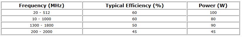
Most radios today support both bands in the same platform so with typical extensions that becomes 30-512 MHz. New wideband data links at 1300 – 1800 MHz mean that a future-proof radio should span 30-2000 MHz and support high peak-to-average linear to CW (constant envelope) waveforms.

LDMOS (laterally diffused metal oxide semiconductor) operates to 2 GHz, but exhibits almost linearly decreasing bandwidth versus frequency. A 30 MHz to 2 GHz radio might require a half dozen or more LDMOS amplifier chains versus only two with GaN devices. Clearly, GaN (Gallium nitride) technology is a new tool for radio designers, one that enables new radio architectures that meet these forward looking bandwidth, efficiency and power density goals.
Why GaN?
GaN is a unique III/V semiconductor process that combines the electron mobility and bandwidth of GaAs, with the high power capability and ruggedness of LDMOS. Compared to LDMOS, a comparable power GaN device has a fraction of the CGS and CDS capacitances. This allows wide bandwidth and high power added efficiency to several GHz with today’s common 0.5 and 0.25 m gate processes.
Within the GaN world there are many suppliers, but only two fundamental recipes, based on either Silicon or Silicon-Carbide substrates. At the top level, both GaN-on-Si and GaN-on-SiC produce a variety of products with similar thermal and RF performance. GaN-on-Si though has a significant cost advantage that, combined with plastic packaging, is disruptively driving down the cost curve. For example; at the 100W level a new GaN-on-Si device has just broken the $1/W barrier in volume, with a roadmap to further reductions as both military and commercial volumes grow. GaN provides the technology breakthrough for wideband operation, but GaN on Si is trimming LDMOS’ principal remaining advantage, i.e. price.
Driver and Mid-level Power Stages
Integrated GaN amplifiers can now address almost any conceivable applications below 2 GHz up to 25W and are easily optimized to meet specific needs. Typical packages include QFN and DFN footprints, with dimensions of 4 to 8 mm per side.
Power amplifiers in the 1W to 10W range find homes as output stages in handheld or battery powered radios, and driver stages in higher power platforms. Because of their varied requirements and moderate volumes, these stages have historically been built around externally matched discrete silicon or GaAs based transistors.
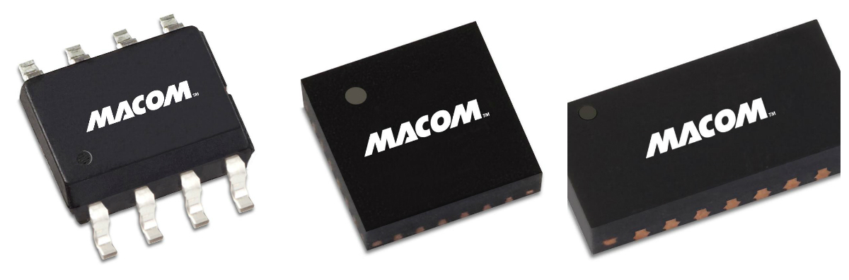
Many GaN devices in this power range still use expensive ceramic packages. But growing volumes allow commercial plastic options that both reduce cost and support standard SMT manufacturing flows. Figure 1 shows typical examples. But designers should exercise some caution with these plastic cased devices as their small footprint pushes a lot of heat into a small circuit board area. While the thermal impedance of the device alone may be surprisingly good, the thermal impedance of the PCB may be a comparable contributor and deserves attention. Good design requires void free solder wetting across the ground pad, a dense array of plated through vias, and in some cases a copper coin either inserted in the board or soldered on the backside. The designer must consider the thermal contribution of every interface and component from the device to the heat-sink or case.
Packages
For these medium power levels new 28V and 48V integrated GaN amplifiers can greatly ease the design task, shrink the board footprint, and deliver better-than-discrete performance. Table 1 offers typical examples, some of which are available from multiple vendors. They combine an integrated input match and a properly sized GaN active device in a reflow friendly plastic or laminate SMT package.
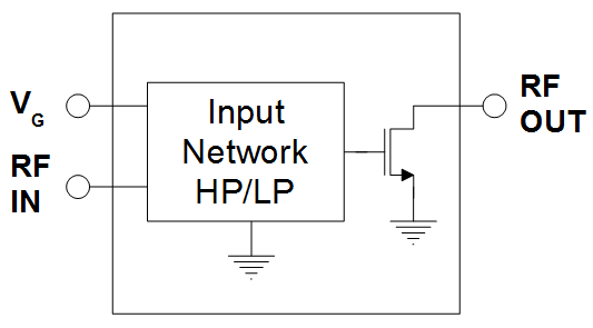
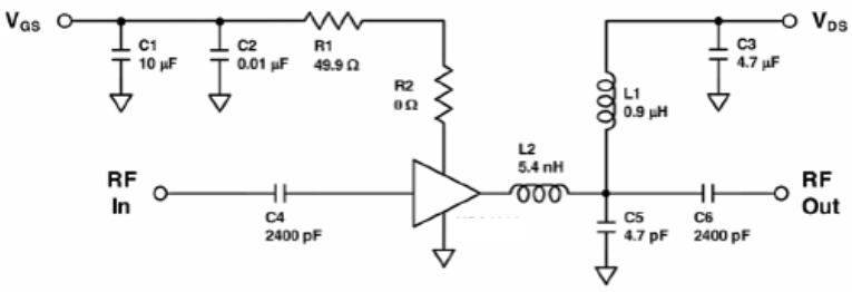
Thanks to the relationship between power voltage and low Q these GaN devices naturally exhibit output impedances that are easily transformed to 50 ohms, especially at low frequencies, so the main design challenge is the higher capacitance, higher-Q, input impedance. The design approach uses a lossy equalizer input match that provides both low VSWR and flat overall gain. Figure 2 shows a simplified functional diagram of a typical device.
The input network includes coupling and bias isolation components that create an inherent low frequency pole. Pay special attention to the data sheet if your lower band edge falls below about 100 MHz as typical 3 dB points fall in the range of 20 MHz to 50 MHz.
While the output is not matched to 50 Ohms, this is easily and efficiently transformed to a 50 Ohm match with a few external SMT passives, sometimes in concert with the bias network as shown in Figure 3. Data sheets usually include wideband or full band application circuits but designers can easily tailor these to maximize power, efficiency, or return loss over narrower bands.
Output Stage
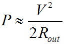
The 50W to 100W power level merits a quick refresher on the relationship between RF power, voltage, and load impedance. Using a 28V supply, the ideal load line for a 100W amplifier is about 4 Ohms using the familiar: