


The second wave of Covid-19 was an unlikely moment to launch a gallium nitride chip, yet AGNIT converted the challenge into momentum and built its first working prototypes within two years. Co-founder Hareesh Chandrasekar notes that the early progress stemmed from disciplined execution during the period of uncertainty. From its pilot facility at IISc, the company runs a vertically integrated line that spans wafer growth to final testing.
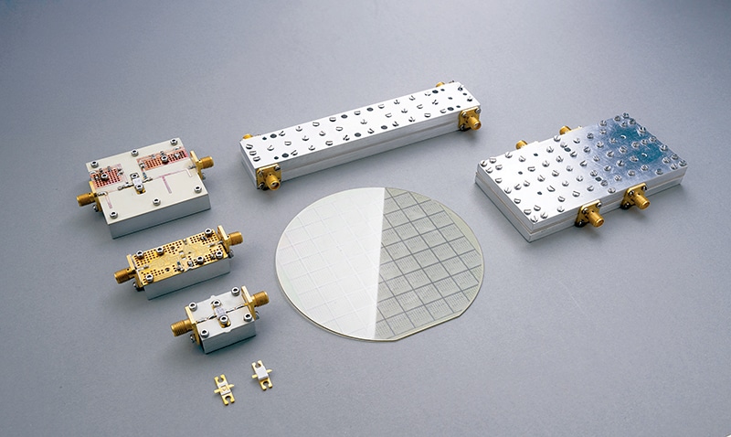
Founded in 2019 and incubated at the Indian Institute of Science (IISc), Bengaluru, AGNIT Semiconductors positions itself as a vertically integrated GaN semiconductor company. The company designs and makes its own wafers, processing them, dicing the chip, assembling, packing, and testing them. Each chip is designed to meet different specifications and is supplied to customers.
“Having technology is one thing, but commercialising it to solve specific customer pain points is quite another,” Chandrasekar says. AGNIT’s markets include defence, space, and telecom, with consumer-facing applications currently under development.

Intellectual property is a central component of the model. The company licenses background IP from IISc and builds its own portfolio, with six applications filed in 2023. Chandrasekar says, “Intellectual property for us is not just patents, it is also trade secrets.” By combining licensed research from IISc with its filings, the company reflects a broader effort to shift India’s role in semiconductors from design services to ownership of core technology.

The company has been operating since the Covid-19 pandemic. Chandrasekar adds, “It was a hard time, especially the second wave. Thankfully, the team stayed together. The period was spent developing, filing patents, and building prototypes.”
By 2022, AGNIT had shipped its first GaN wafers and developed initial RF amplifier prototypes, marking its transition from a research entity to a functioning semiconductor enterprise. These early prototypes targeted high-frequency GaN chips, particularly in telecom base stations and defence radar systems, where high power density and efficiency are critical.
“Our first focus was to prove that India could build world-class GaN RF devices,” says Chandrasekar. “Once that was validated, the focus shifted to scaling.”
AGNIT’s core product line today includes:
• GaN epitaxial wafers: Custom-grown GaN films on silicon and silicon carbide
• GaN RF devices: High-efficiency transistors and amplifier modules for telecom, radar, and aerospace applications, covering frequencies from S-band to X-band
• Evaluation boards and modules: Ready-to-use boards that help customers test and integrate AGNIT’s devices faster
In December 2023, AGNIT signed a contract under the iDEX (Innovations for Defence Excellence) programme of India’s Ministry of Defence. The partnership supports the development of indigenous GaN components for radar and electronic warfare systems.
“For decades, silicon has been the default semiconductor material. However, GaN offers distinct physical properties. It provides about five times higher electron mobility and can withstand roughly three times the voltage of silicon before failing,” he informs.
It conducts electricity very efficiently when switched on and blocks high voltage when switched off. At the same time, it conducts heat more effectively and can be built in a small, compact form.
AGNIT runs its production inside the IISc facility, using a small-volume GaN foundry supported by the Ministry of Electronics and IT (MeitY). It allows startups to access advanced fabrication without the massive investment required for commercial labs.
“When people tell you they need 20 billion dollars to set up a silicon fab, a team could spend 500 million dollars and set up a reasonably sized gallium nitride fab,” Hareesh Chandrasekar discloses.
Manufacturing GaN chips differs significantly from manufacturing silicon chips. Native GaN wafers are extremely difficult to make compared to silicon substrates, so GaN is typically deposited on silicon wafers, sapphire wafers, or silicon carbide wafers. LEDs often use sapphire because it is transparent.
“Our RF components are built on silicon carbide due to its thermal conductivity. Fast chargers rely on GaN on silicon because it is cost-effective,” he says.
Funding and talent remain key hurdles. Developing semiconductors requires patient capital, often for years before revenue is generated. “There is not much VC money for semiconductors. Grants and government funds become essential,” Chandrasekar says. The company also faces the challenge of building specialised expertise in India, where most semiconductor jobs traditionally centre on design services for multinationals.
Parallel to the RF chips, AGNIT is pushing its GaN product segment beyond defence and telecom into power electronics. The team is experimenting with GaN-powered EV chargers for their compact and fast-charging capabilities. “We are still testing; the potential is massive. If this scales, the next EV charger could fit in a backpack, smaller, faster, and far more efficient than anything silicon can do today.”