Ultra-thin MOS transistors using advanced materials engineering, enabling higher transistor density, lower power consumption, and improved performance for future AI, mobile, and computing chips.
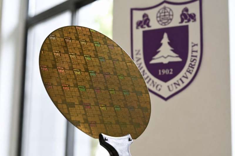
A research team has demonstrated a new generation of ultra-thin metal-oxide-semiconductor (MOS) transistors that could help extend chip scaling beyond the limits faced by conventional silicon technologies. The breakthrough addresses one of the semiconductor industry’s biggest challenges: maintaining transistor performance as devices shrink to increasingly smaller dimensions.
The development centers on transistors built with atomically thin semiconductor channels, allowing engineers to reduce device size while preserving electrical control. As chipmakers pack more transistors onto a single die to improve computing performance, traditional transistor architectures face rising leakage currents, heat generation, and power inefficiencies. The newly developed design aims to overcome these constraints by leveraging ultra-thin materials that provide stronger gate control over electron flow.
According to the researchers, the transistors demonstrate key performance metrics required for future logic chips, including efficient switching behavior and reduced power loss. The architecture also supports aggressive scaling, making it suitable for next-generation processors used in artificial intelligence, high-performance computing, and mobile devices.
A major advantage of the approach is its compatibility with advanced semiconductor manufacturing strategies. Rather than relying solely on shrinking silicon structures, the technology introduces new channel materials and device engineering techniques that can sustain performance improvements as transistor dimensions continue to decrease.
The achievement comes as the semiconductor industry searches for alternatives to conventional scaling methods. With leading-edge chip production approaching physical and economic limits, researchers worldwide are exploring two-dimensional materials, novel transistor structures, and advanced packaging technologies to maintain progress in computing performance.
If successfully integrated into commercial fabrication processes, the ultra-thin MOS transistors could enable denser chips with lower energy consumption and higher processing capability. Such improvements would be particularly valuable for AI accelerators and data-center processors, where power efficiency has become as important as raw computational speed.
While further work is required before large-scale manufacturing, the results demonstrate a promising pathway for extending transistor innovation into future technology nodes. The research highlights how material science and device engineering are increasingly shaping the next era of semiconductor advancement.