


The AI industry has spent years scaling models through brute-force computing. HC1 takes a different path entirely, collapsing hardware and software into a single architectural layer.
A radical compute-in-memory architecture is collapsing the boundary between hardware and AI models, eliminating data movement and redefining performance-per-watt. The HC1 by Taalas is not just faster, it signals a fundamental shift in how chips are conceived, built, and optimised for the next era of AI inference.
The unveiling of the HC1 is not merely another addition to the crowded AI chip market—it represents a fundamental rethinking of how artificial intelligence workloads are executed. HC1 addresses inefficiencies in current AI infrastructure by targeting escalating costs, rising energy demands, and architectural bottlenecks that are beginning to constrain large-scale AI deployment.
At its core, the HC1 introduces a new category of compute hardware in which AI models are no longer software artefacts running on general-purpose processors. Instead, they are physically instantiated into silicon. This shift effectively turns the chip into the model itself, collapsing the distinction between hardware and software while enabling performance levels that exceed current inference benchmarks.
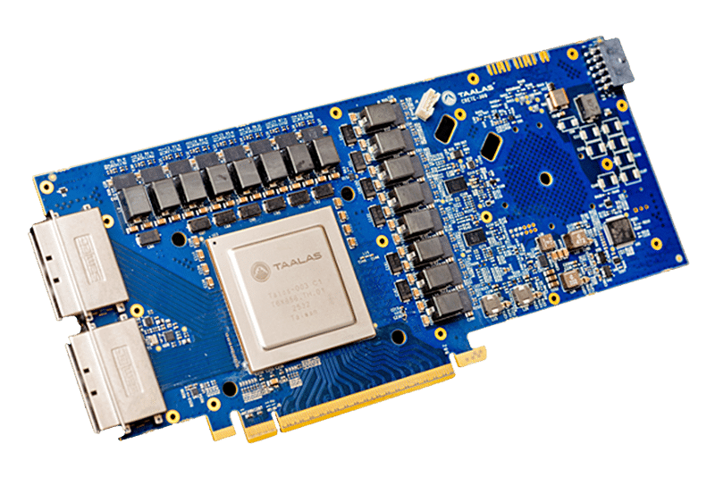
The company claims the HC1 achieves throughput of 17,000 tokens per second on Llama 3.1 8B—an order-of-magnitude leap over existing systems. Crucially, this performance is delivered without reliance on high-bandwidth memory (HBM), liquid-cooling systems, or hyperscale infrastructure. A fully configured server equipped with ten HC1 cards operates at approximately 2.5kW using standard air cooling, dramatically lowering the barrier to deployment.
The infrastructure crisis driving innovation
The HC1 emerges against the backdrop of a growing crisis in AI infrastructure, where traditional system architectures are struggling to keep pace with demand. The central issue lies in the ‘memory wall’—a long-standing limitation in computing where data transfer between memory and processing units becomes the dominant bottleneck.
In conventional AI systems, compute units such as GPUs are physically separated from memory. Each inference operation requires continuous movement of model weights and intermediate data across this boundary. This process is not only time-consuming but also highly energy-intensive, with estimates suggesting that 80-90% of total energy consumption is spent on data movement rather than arithmetic itself, a figure increasingly validated by real-world data centre telemetry.
These inefficiencies manifest as increased latency, excessive heat generation, and the need for complex cooling and infrastructure systems. Even the most advanced chips today, delivering fewer than 2000 tokens per second, are increasingly inadequate for real-time, large-scale AI applications.
Eliminating data movement through architectural convergence
HC1 addresses this challenge with a radical architectural approach: eliminating data movement entirely by removing the separation between compute and memory.
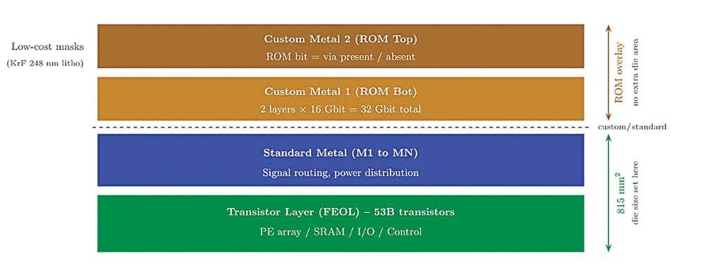
In the HC1, the full Llama 3.1 8B model is hardwired directly into the chip using a mask-ROM-based recall fabric. This design ensures that model weights are permanently embedded within the silicon, removing the need to fetch data from external memory during inference. Key results:
- Sub-millisecond latency
- Dramatically improved energy efficiency
- No dependence on external memory hierarchy
A crucial but often overlooked implication is that this architecture converts memory access into constant-time lookup, eliminating cache hierarchies, DRAM stalls, and bandwidth contention entirely, one of the deepest sources of unpredictability in modern AI systems.
| Taalas—Where AI becomes silicon |
| Taalas is a US-based semiconductor startup founded in 2023. The company is redefining AI computing through its model-as-silicon architecture, in which neural networks are integrated directly into computer chips rather than run through software. The company’s flagship product, the HC1, employs a compute-in-memory design that eliminates data movement, delivers superior performance per watt, and simplifies deployment by using standard air cooling rather than a high-bandwidth memory infrastructure. By locking down much of the model while retaining only an adaptable layer, Taalas has struck a balance between extreme efficiency and practical deployment. Its strategy centres on two key areas: first, compiling AI models directly into silicon while removing memory bottlenecks to accelerate performance; and second, delivering high-efficiency inference hardware supported by simplified, scalable AI infrastructure. Taalas represents a broader shift towards purpose-built intelligence hardware, where chips are designed around AI models rather than the other way around. |
What makes the HC1 unique
The HC1 architecture is built around a unified compute-memory cell, in which a single transistor can store data and perform multiplication simultaneously. This integration effectively collapses traditionally separate components, such as memory arrays, multiply-accumulate (MAC) units, and interconnect layers, into a single structure.
A key quantitative insight: instead of shuttling weights across millimetres of interconnects, as in GPUs, computation happens in place at the bit-cell level, reducing data movement distance by orders of magnitude, from millimetres to nanometres.
Complementing this is the mask-ROM recall fabric, in which model weights are encoded directly during chip fabrication. This approach enables:
- Multi-bit storage (~4 bits per cell typical)
- Near-zero read energy
- Deterministic latency (no cache misses, no bandwidth contention)
Unlike SRAM or DRAM, mask ROM has effectively zero standby power and extremely high density, making it ideal for inference workloads where weights remain static.
| HC1 vs Traditional hardware | ||
| Feature | Traditional GPU/Accelerator | HC1 |
| Model location | External memory | Hardwired in silicon |
| Data movement | High | Eliminated |
| Energy usage | High (memory dominated) | Low |
| Cooling | Liquid/advanced | Air-cooled |
| Flexibility | High | Limited |
| Throughput | <2000 tokens/sec | ~17,000 tokens/sec |
The hybrid layer: Where flexibility still exists
Despite being largely fixed, HC1 incorporates a hybrid dynamic layer, which is critical to its practicality. This SRAM-based subsystem supports:
- KV caching for transformer inference
- LoRA-style fine-tuning overlays
- Adjustable context windows
This is a subtle but crucial design choice. Rather than making the entire model programmable, HC1 keeps 95% of computation fixed and optimises the remaining 5% for adaptability—a trade-off that captures most efficiency gains without rendering the system unusable. While 17,000 tokens/sec is headline-grabbing, deeper analysis suggests:
- Performance gains come primarily from eliminating memory bottlenecks, not dramatically faster arithmetic
- Effective throughput depends heavily on:
- Quantisation level (e.g., 4-bit vs 8-bit)
- Batch size assumptions
- Sequence length and KV cache reuse
In other words, HC1’s advantage is structural, not just computational. It removes the dominant bottleneck rather than marginally improving compute units.
System-level advantages
At the system level, HC1 introduces several second-order benefits that are often underestimated:
- No HBM→no memory bandwidth bottleneck
- No large interconnect fabric→ reduced latency variance
- No liquid cooling→ a dramatically simpler deployment
- Linear scaling with cards→ predictable cluster performance
This leads to a key economic shift: AI infrastructure moves from bandwidth-constrained scaling to compute-density scaling.
Engineering trade-offs and hidden costs
While the HC1 architecture is highly innovative, it introduces significant constraints:
1. Model immutability
Updating weights requires new silicon. This creates:
- Long iteration cycles (months vs days)
- Tight coupling between the model lifecycle and fabrication
2. Manufacturing complexity
Mask-ROM-based designs:
- Increase tape-out rigidity
- Require near-perfect model finalisation pre-fabrication
- Introduce yield risks if defects affect encoded weights
3. Toolchain reinvention
HC1 effectively creates a new stack:
- Modelsilicon compilers
- Hardware-aware quantisation pipelines
- New debugging paradigms (you can’t ‘print logs’ from silicon)
4. Precision constraints
Most such systems rely on low-bit quantisation (≈4-bit), which:
- Works well for many LLMs
- But it may degrade accuracy in edge cases
For engineers, HC1 represents a deeper paradigm shift:
- Compute-in-memory becomes practical, not theoretical
- Software-hardware co-design becomes mandatory
- ASIC workflows evolve into model compilation pipelines
The biggest conceptual change: You no longer deploy models onto hardware; you fabricate hardware from models.
The HC1 architecture lends itself to:
- Data centres: High-throughput inference with lower energy footprint
- Enterprise AI: Predictable, cost-efficient deployments
- Edge AI (future): Real-time inference with minimal power budgets
Market implications and investment momentum
HC1 arrives at a pivotal moment when AI inference demand is rapidly accelerating, GPU supply remains constrained, and energy consumption is emerging as a primary limiting factor in scaling AI systems. Its positioning as a cost-per-token disruptor is rooted in a fundamentally different approach: eliminating the energy overhead of memory movement, removing dependence on high-bandwidth memory, and simplifying overall system architecture. These advantages not only improve efficiency but also catalyse broader industry interest in model-specific silicon, compute-in-memory designs, and domain-specific AI accelerators.
More importantly, HC1 does not represent an incremental step forward; it inverts the traditional compute paradigm. Instead of running models on chips, it embodies a model-as-chip architecture in which software is effectively integrated into hardware. This shift trades flexibility for substantial efficiency gains and replaces bandwidth-driven scaling with structural optimisation at the silicon level. If this approach proves scalable, it has the potential to disrupt a landscape long dominated by GPUs and general-purpose accelerators, offering a fundamentally new blueprint for computation.
In this sense, HC1 signals a decisive transition from programmable, general-purpose computing towards fixed, purpose-built intelligence hardware. For engineers, the implication is profound: the boundary between model and machine is rapidly dissolving, and future chip design may increasingly begin not with transistors, but with neural network architectures themselves.
Akanksha Sondhi Gaur is Senior Technology Journalist at EFY with a German patent to her credit. She has seven years of industrial and academic experience, and has penned several research papers.