
The global electric vehicle charging station market size is projected to reach 30,758 thousand units by 2027, from an estimated 2,115 thousand units in 2020, at a CAGR of 46.6%. The base year for the report is 2019 and the forecast period is from 2020 to 2027 (source Markets and Markets., February 2021).
Geographically, rapidly growing sales of electric vehicles in the Asia Pacific region, especially in China, has propelled the growth of the global market for electric vehicle charging stations. Europe is expected to be the second-largest market during the forecast period.
Considering the various charging level types, the Level 3 charging type (i.e. DC fast charging) is expected to grow fastest during the forecast period. Level 3 charging has been growing at the quickest rate due to the convenience of fast charging EVs within 30 minutes. STMicroelectronics’ products support this market/application. We’ll take a look at the main system architectures and the main suitable ST products in the following sections.

Architectures and ST’s Products
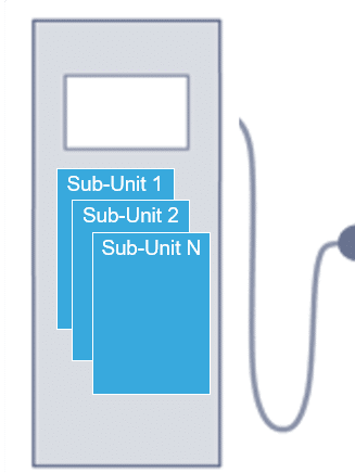
The power range for DC fast chargers covers 30-150kW and implements a modular approach (fig.1) based on 15-30 kW subunits, which are then stacked up to create the higher power DC charging system. This approach provides a flexible, fast, safe and affordable solution.
ST’s products cover the main power and control unit/driving stages included in each sub-unit (fig.2).
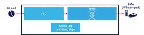
Concerning the power stage (PFC + DC-DC sections), design efficiency is the key, and for a sub-unit of 15-30kW power range, ST offers suited, efficient and smart products for PFC, DC-DC and Control unit/driving stages, as reported in the following sections.
PFC stage
The power factor correction (PFC) stage, for a 3-phase input, can be implemented through several configurations, and often Vienna rectifier topologies are used (fig.3, type 1 or type2).
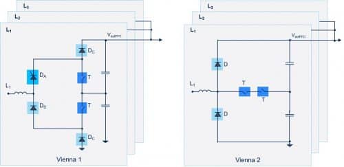
Based on the design and/or customer needs, ST offers a wide variety of switches (fig.3, device T):
⦁ SiC MOSFETs Gen 2 (650V series SCT*N65G2) is based on the advanced and innovative properties of wide bandgap materials and feature very low Rdson per area that combined with excellent switching performance provides an efficient and compact design. In particular, the 4-pin SCTW90N65G2V-4 with its 18mΩ RDS(on), can comfortably handle 90 A of drain current at 100°C.
⦁ IGBTs HB2 series (650V family STGW*H65DFB2) ensures higher efficiency in applications working at medium to high frequencies. Combining both lower saturation voltage (1.55 V typ.) and lower total gate charge, this IGBT family ensures minimal overshoot voltages during turnoff as well as lower turn-off energy in application. In particular, the STGW40H65DFB-4 provides faster switching thanks to a Kelvin pin that separates power path and driving signal.
⦁ Power MOSFETs MDMesh M5 series (650V family, STW*N65M5)uses an innovative vertical process to have a higher VDSS rating and high dv/dt capability, outstanding RDSon x area, and excellent switching performance.
In the input stage, it is possible to control the inrush current with these devices:
⦁ SCR Thyristors TN*50H-12WY (fig.3, Vienna 1, device DA), an AEC-Q101 qualified rectifier, offers 1200V blocking capability with an optimised power density and surge current capability. In this way, it is possible to avoid the use of passive components that limits the efficiency and lifetime of the system.
⦁ Rectifiers for the input bridge, the STBR*12 1200 family (fig.3, Vienna1, device DB) with its low forward voltage drop improve the efficiency of the input bridges in compliance with the most stringent standards. That products are ideal for use in mixed-bridge configurations along with ST’s SCR Thyristor.
As far as diodes are concerned, the topologies of the new SiC Diodes 650/1200V series combines the lowest forward voltage with state-of-the-art forward surge current robustness. Designers can select a lower current rating diode without compromising the converter’s efficiency level while increasing the affordability of high performing systems.
⦁ 650V (STPSC*H65) on Vienna type 1 (fig.3, device DC)
⦁ 1200V (STPSC*H12) on Vienna type 2 (fig.3, device D)
DC-DC stage
In the DC-DC conversion stage, a full bridge resonant topology (fig.4) is often preferred due to its efficiency, galvanic isolation and fewer devices.
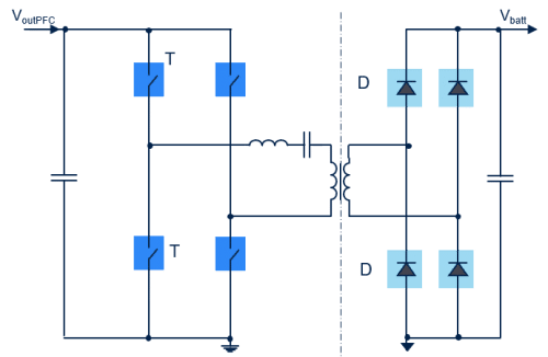
Considering a 3-phase PFC converter with Vout= 750-900V, and a HV battery of 400V-800V, for FB-LLC resonant converter ST proposes:
⦁ SiC MOSFETs Gen 2 1200V series SCT*N120G2 (fig.4, device T)
⦁ SiC Diodes 1200V STPSC*H12 (fig.4, device D)
Control unit and driving stage
Depending on the needs of the design, ST offers both MCUs and digital controllers:
⦁ The 32-bit microcontrollers most suitable for power management applications are the STM32F334 (from the STM32F3 family) and the STM32G474 (from the STM32G4 family). The STM32F3 MCU series combines a 32-bit ARM Cortex-M4 core (with FPU and DSP instructions) running at 72 MHz with a high-resolution timer and complex waveform builder plus event handler. The STM32G4 series’ 32-bit ARM Cortex-M4+ core running at 170 MHz is a continuation of the STM32F3 series, maintaining the series’ leadership in analogue that grants cost reduction at the application level, a simplification of the application design, and the chance for designers to explore new segments and applications.
⦁ The heart of the STNRG388A digital controller is the SMED (State Machine Event Driven), which allows the device to pilot six independently configurable PWM clocks with a maximum resolution of 1.3 ns. Each SMED is configured via the STNRG internal microcontroller. A set of dedicated peripherals complete the STNRG device: 4 analogue comparators, 10-bit ADC with configurable op-amps and an 8-channel sequencer. and a 96 MHz PLL for high output signal resolution.
The new STGAP2SICS is a 6kV galvanic isolated single gate driver designed to drive SiC MOSFETs. It features a 4A sink/source current capability, short propagation delay, up to 26V supply voltage, optimized UVLO and standby function, and a SO8W package.
ST’S Evaluation Boards
For just about any application type, ST offers the right system evaluation boards for testing features of ST’s products directly in the final system or sub-system. For the DC charging station, some boards and related firmware are available as well.
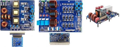
The STDES-VIENNARECT evaluation board (fig.5-a) features a 15 kW, three-phase Vienna rectifier with mixed-signal control for the power factor correction (PFC) stage.
The high switching frequency of the SCTW35N65G2V 650V SiC MOSFETs (70 kHz), the adoption of STPSC20H12 1200V SiC diodes, and the multilevel structure allows nearly 99% efficiency as well as the optimization of passive power components in terms of size and cost. The STEVAL-VIENNARECT features mixed-signal control, with the STNRG388A controller providing digital output voltage regulation. Dedicated analogue circuitry provides high bandwidth continuous conduction mode (CCM) current regulation for maximum power quality in terms of total harmonic distortion (THD<5%) and power factor (PF>0.99).
The STDES-VIENNARECT evaluation board (fig.5-a) features a 15 kW, three-phase Vienna rectifier with mixed-signal control for the power factor correction (PFC) stage. The high switching frequency of the SCTW35N65G2V 650V SiC MOSFETs (70 kHz), the adoption of STPSC20H12 1200V SiC diodes, and the multilevel structure allows nearly 99% efficiency as well as the optimization of passive power components in terms of size and cost. The STEVAL-VIENNARECT features mixed-signal control, with the STNRG388A controller providing digital output voltage regulation. Dedicated analogue circuitry provides high bandwidth continuous conduction mode (CCM) current regulation for maximum power quality in terms of total harmonic distortion (THD<5%) and power factor (PF>0.99).
The STDES-PFCBIDIR evaluation board (fig.5-b) features 15 kW, three-phase, three-level Active Front End (AFE) bidirectional converter for power factor correction (PFC) stage. The power side adopts SCTW40N120G2VAG 1200V SiC MOSFETs which guarantee high efficiency (nearly 99%). The control is based on the STM32G4 series microcontroller with connectors for communication, and test points and status indicators for testing and debugging. The driving signals for the switching devices are managed by corresponding STGAP2S gate drivers to ensure independent management of switching frequencies and dead time.
The STEVAL-DPSTPFC1 3.6 kW bridgeless totem pole boost circuit (fig.5-c) achieves a digital power factor correction (PFC) with a digital inrush current limiter (ICL). It helps you to design an innovative topology with the latest ST power kit devices: a silicon carbide MOSFET (SCTW35N65G2V), a thyristor SCR (TN3050H-12WY), an isolated FET driver (STGAP2S) and a 32-bit MCU (STM32F334).
The author works as Technical Marketing Manager at STMicroelectronics.