GPS and GSM modules are among the most widely used and essential components for designing and prototyping GPS trackers and cellular IoT systems.
However, most of these modules are costly and often come as separate units. If your design requires both functionalities, you need to purchase two separate modules, which increases the overall design cost and impacts the bill of materials (BOM).
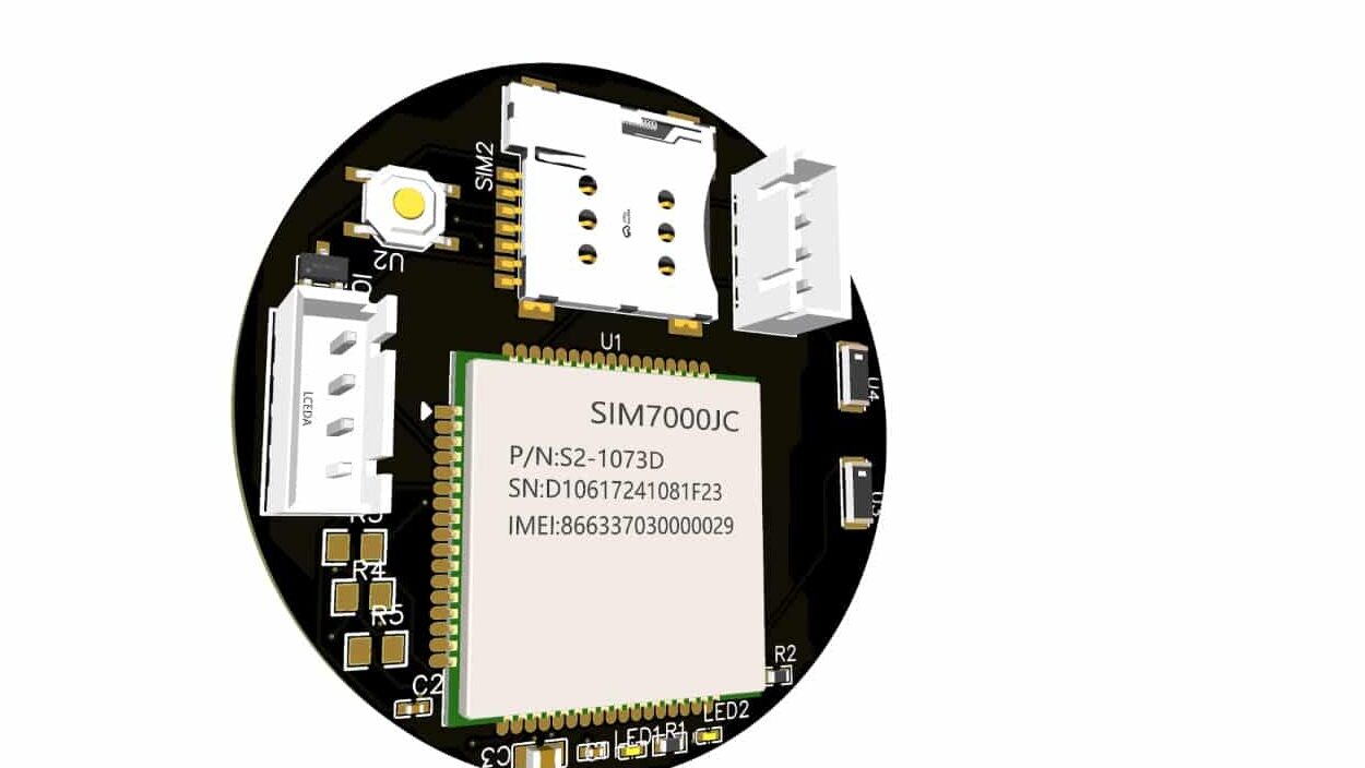
Additionally, these modules are typically large, making them unsuitable for miniature and compact designs where size is a critical factor. To address this, we have designed the smallest 3 cm-sized GPS and GSM module integrated into a single chip.

This solution simplifies prototyping and design of compact GPS trackers and cellular IoT systems.
The best part? The hardware is completely open-source, allowing you to modify the design and adapt it for your personal projects as needed. We have provided the complete bill of materials, schematics, and PCB design in the open-source domain.
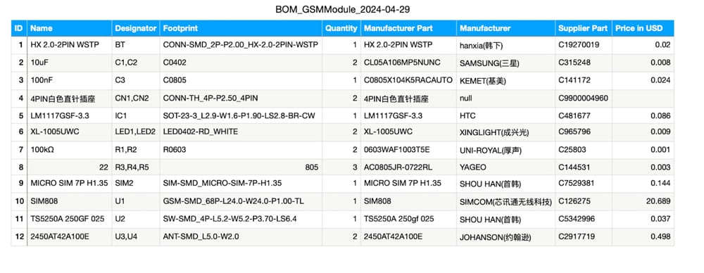
Bill of Materials
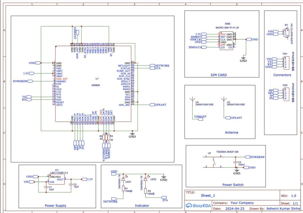
Designing GSM + GPS Module
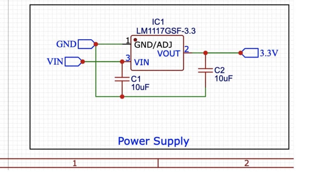
Power System
Here for the power system, we use the LDO voltage regulator IC of 3.3V because the chip needs the same range of voltage input and and so here we use LDO that gives us output voltage around 3.3V with current ranging from 800mA to 1A. The LDO IC needed the two capacitors at the input and output.
The LDO regulator requires minimal external components, making it ideal for a compact design. The circuit includes:
- Input Capacitor: A 10 µF ceramic capacitor at the LDO’s input to stabilize the input voltage and filter noise. This capacitor is placed close to the input pin to minimize trace inductance.
- Output Capacitor: A 10 µF ceramic capacitor at the LDO’s output to ensure stability and reduce output voltage ripple. The capacitor’s low ESR (Equivalent Series Resistance) enhances performance.
- LDO IC: The core regulator, converting an input voltage (e.g., 3.6V–5V from a battery or external supply) to a stable 3.3V output.
- Bypass Resistors (Optional): Depending on the LDO model, a small resistor may be included for thermal protection or current limiting.
The input voltage can be sourced from a 3.7 V LiPo battery or a 5V external supply, commonly used in IoT prototyping. The LDO’s low dropout voltage ensures efficient operation even when the input voltage is close to 3.3V.
Indicators
Here, the chip we are using provides two indicating options to indicate the network and GPS status. So we add the LD with a 1K resistor with those indicator pins on the chip.


Subsequently, we incorporate the antenna here. You can modify the design to accommodate an on-board antenna, a UFL antenna connector, but in this instance, I have utilized an SMD antenna with a size of 1 cm.
Next, we employ a simulation slot and connect the communication peripheral pins with the chip pins. Finally, we add the connector for accessing and communicating with the GPS and GSM module.
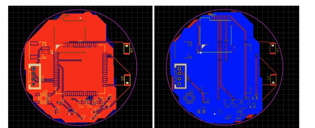
PCB Design for Tiny 3cm GPS and GSM Module
Now we will design the PCB and place components as per your wish. Here I have designed the PCB in a 3 cm size.
Also, previously, we built the Smallest Open-Source LoRa + GPS Module for Wearables and IoT. You can check it too.