
Designed by Hans Camenzind in 1971, the NE555 timer IC went on to become one of the most widely manufactured electronic components ever made. Originally designed to replace bulky and unreliable discrete RC circuits, the NE555 quickly proved far more versatile than expected. Engineers worldwide deployed it in oscillators, pulse-width modulators, tone generators, missing pulse detectors, voltage-controlled oscillators, and hundreds of other applications. More than five decades later, it remains one of the most successful ICs ever created, with over a billion units still manufactured every year.
The genius of the 555 timer lies in its simple internal topology. At its core, the device consists of three equal resistors forming a precision voltage divider between VCC and GND, creating two stable reference voltages at 1/3VCC and 2/3VCC. These references feed two analogue comparators — an upper comparator monitoring the threshold pin (pin 6) against 2/3 VCC, and a lower comparator monitoring the trigger pin (pin 2) against 1/3 VCC. The outputs of these comparators drive an SR latch, whose complemented output controls both an open-collector discharge transistor (pin 7) and the output stage (pin 3). A reset pin (pin 4) provides asynchronous override capability, and a control voltage pin (pin 5) allows external modification of the comparator reference levels — a feature often overlooked but enormously powerful in FM and PWM applications.
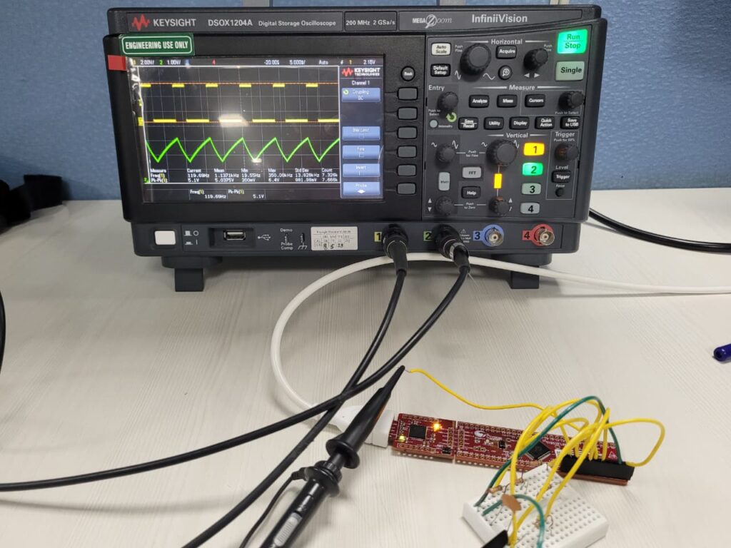
PSOC 4: A canvas for analogue and digital co-design
Unlike convenient microcontrollers, which come with fixed hardware peripherals, Infineon Technologies’ PSOC 4 (Programmable System-on-Chip) allows engineers to configure both analogue and digital hardware to suit their application. Instead of writing firmware to imitate a circuit, designers can recreate the circuit itself inside the chip. This unique capability makes PSOC 4 an ideal platform for rebuilding the classic NE555 timer.
To recreate the 555, the project uses several configurable hardware blocks available in the PSOC 4. The analogue subsystem includes two low-power comparators (LPCOMPs) that replicate the threshold and trigger detection of the original timer, while the Universal Digital Blocks (UDBs) implement the SR latch entirely in hardware. A programmable digital interconnect links these blocks together, closely mirroring the signal flow inside the original NE555 without relying on CPU intervention. Additional resources, including four OpAmps, a 12-bit SAR ADC and two CAPSENSE blocks, offer further flexibility for extending the design.
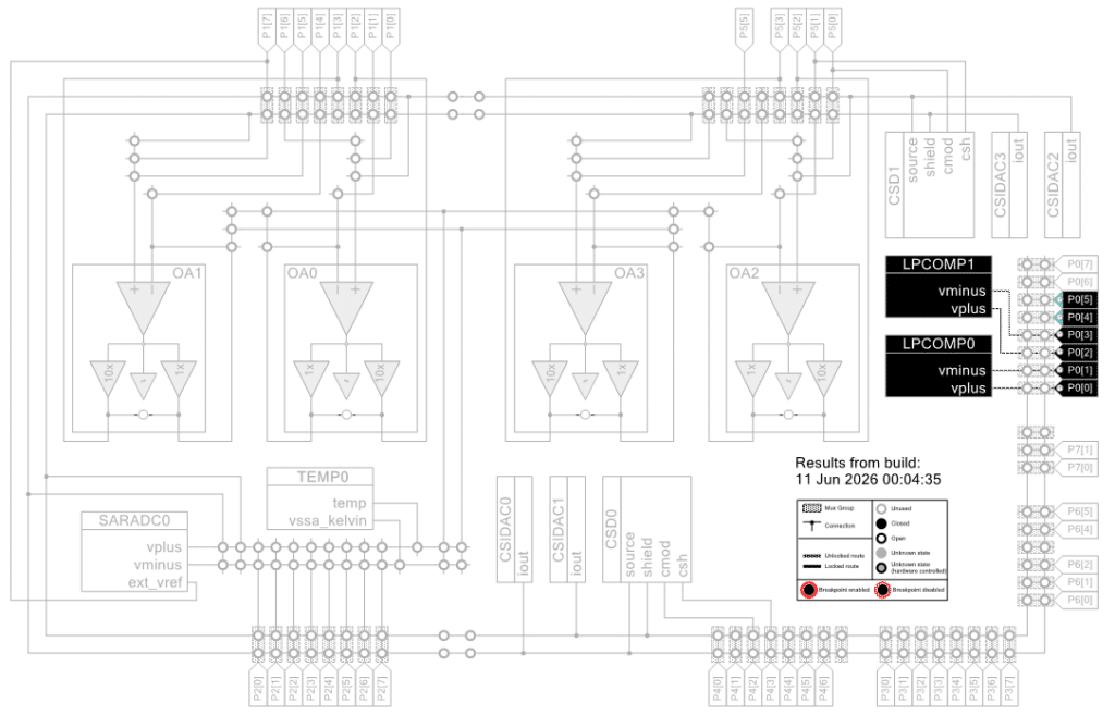
Reconstructing the voltage divider and comparators
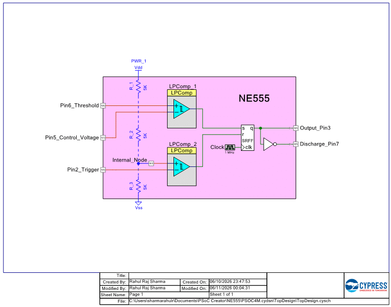
In the original NE555, a simple resistor ladder generates two fixed reference levels at 1/3 VCC and 2/3 VCC. In this project, the same behaviour is recreated in two possible ways. A straightforward approach uses an external network of three 5 kΩ resistors to form the divider, while a more flexible implementation can leverage the PSOC 4’s internal current DACs to generate precise reference voltages without relying on discrete components.
These reference levels are then fed into the PSOC 4 comparator inputs, while the trigger and threshold signals are routed through GPIO pins to the appropriate comparator terminals. This configuration directly mirrors the behaviour of the original NE555, where one comparator responds to the trigger input below 1/3 VCC and the other monitors the threshold crossing above 2/3 VCC.
One advantage of implementing this structure in PSOC 4 is speed and configurability. The other available resources within the PSOC 4 can be used to build a more complex application and reconfigure the internal logic of NE555 in ways it was never possible before.
SR latch implementation in the UDB
The heart of the 555’s logic is the SR latch, and in PSOC 4 this is implemented inside the Universal Digital Block. This is the unique capability of PSOC 4 to implement an actual digital flip-flop within a device, the final building block of a 555 chip. The Set input is driven by the threshold comparator output (active when Threshold > 2/3 VCC) and the Reset input is driven by the trigger comparator output (active when Trigger < 1/3 VCC).
This entire latch structure executes in hardware without consuming CPU clock cycles, ensuring that the timing behaviour is deterministic and not subject to interrupt latency — a critical requirement for accurate pulse generation. The UDB-based latch achieves toggling speeds well into the MHz range, again comparable to the original bipolar implementation. The only code required to implement this design is just two lines to initialise the two comparators (See below).
#include "project.h"

int main(void)
{
    /* Initialize the global interrupts */
    CyGlobalIntEnable;

    /* Initialize the comparators */
    LPComp_1_Start();
    LPComp_2_Start();
    for(;;)
    {
        /* Place your application code here. */
    }
}
Discharge transistor and output stage
In the original NE555, an internal NPN transistor connected to pin 7 provides the discharge path for the external timing capacitor. When activated, it pulls the discharge node to ground, allowing the capacitor to reset during each timing cycle.
In the PSOC 4 emulation, this function is replicated using a GPIO pin configured in open drain mode. The pin is driven directly from the complementary output of the UDB-based SR latch through the digital routing fabric. This preserves the original logic behaviour, where the discharge path becomes active when the latch output is low and is disabled when the output is high.
The main output (pin 3 equivalent) is implemented using a standard push-pull GPIO driven by the Q output of the latch, capable of sourcing and sinking current appropriate for LED or logic-level drive applications.
Timing accuracy and calibration advantages
One significant advantage of the PSOC 4 emulation over the classical 555 is calibration capability. The original NE555 specifies the internal resistor divider with tolerances that can vary the 1/3 and 2/3 VCC thresholds by several percent across temperature and process variations — directly affecting timing accuracy. In the PSOC 4 implementation, the reference voltages are derived using the external resistances, allowing to use highly precise resistances providing much better timing accuracy across temperature and input voltage variations. We can also use the internal IDACs to generate a precise reference for these comparators and adjust the thresholds anywhere we like rather than using 1/3 VCC and 2/3 VCC.
When legacy meets programmability
What makes this emulation project valuable for engineering students is not just the recreation of a 50-year-old IC, but the insight it offers into both classic analogue design and modern reconfigurable hardware. The NE555 remains widely taught because its architecture demonstrates true functional minimalism. Rebuilding it inside PSOC 4 provides hands-on exposure to comparator-based threshold detection, SR latch operation and RC timing fundamentals.
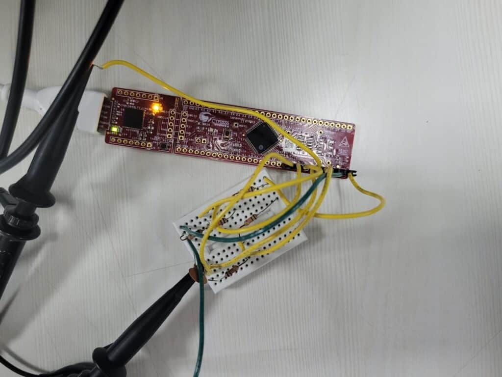
Beyond replication, the PSOC 4 platform also extends what the original NE555 could achieve. The control voltage node can be dynamically driven using an onboard DAC to enable frequency modulation techniques that were not part of the original design space. The ARM Cortex M0+ core can monitor timing behaviour and compensate for drift in real time, while multiple independent 555-style instances can be implemented on a single device using separate comparator and UDB resources, something that would have required multiple discrete ICs in traditional implementations.
The NE555 showed that remarkable versatility can emerge from a simple architecture. PSOC 4 demonstrates how that same architecture can be recreated, expanded, and adapted in a programmable environment. Together, they highlight enduring principles of analogue and digital design that continue to remain relevant on the bench today.