


 The tuning of a frequency modulated (FM) receiver to a FM radio station frequency involves a lot of ‘hissing’ noise in between the stations, which is very irritating for the operator and as such undesirable. Digital FM receivers are free from this problem, because in them the output is automatically clipped during off-station gaps. However, digital FM receivers are comparatively much costlier than their analogue counterparts.
Analogue FM receivers employ an LC tuning system that generates ‘hiss’ noise at the output, which remains unclipped during off-station tuning. However, when the received signal level is adequate (i.e., when the receiver frequency is very close to an FM transmitting station frequency), the limiter circuit preceding the ratio detector circuit in an analogue FM receiver will clip/limit any noise riding the FM carrier.
The simple noise muting FM receiver circuit described here eliminates this ‘hissing’ noise from the output of an analogue FM receiver circuit when it is not resonating to any FM transmitting station’s frequency. In other words, this circuit mutes the output from an analogue FM receiver when its tuner circuit is sweeping in between FM stations.

Circuit Description
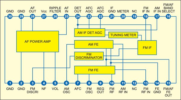
The noise muting FM receiver circuit has been configured around a Sony CXA1619S AM/FM receiver chip, which is available in a 30-pin PDIP package. Sony FM receiver chips are known for their superior features and cost-effectiveness. The functional block diagram of the chip is shown in Fig. 1.
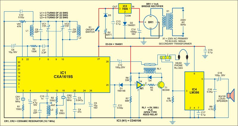
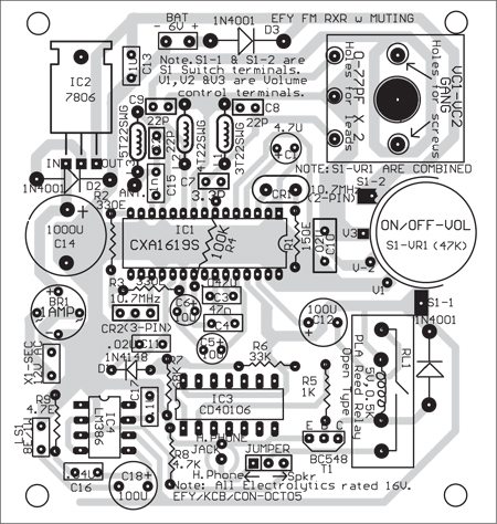
A complete circuit of the FM receiver including the muting circuit and power supply is shown in Fig. 3. Most of the FM kits available in the market also make use of Sony CXA1619S, which is a complete AM/FM receiver IC with very few external components. It can operate at voltages as low as 3V. Here, we have used a 6V supply so that we can feed the output of the receiver directly to a 32-ohm headphone or to a low-power AF amplifier built around IC LM386. A 3-pin jumper has been provided to enable the desired selection.

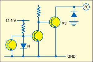
The muting circuit makes use of the tuning meter output at pin 20 of CXA1619S. The internal circuit around pin 20 of the chip is shown in Fig. 2. Normally, this pin is used for tuning indication using a light-emitting diode (LED). The cathode of the tuning indicator LED is connected to pin 20, while the anode of the LED is connected to positive supply through a current limiting resistor.
When the receiver is tuned to the centre of FM carrier, pin 20 of CXA1619 goes very low and the LED lights up the brightest.
Circuit connections
Instead of connecting an LED, we have coupled pin 20 of CXA1619S to the input of a CMOS inverter gate via diode D1. In ‘off’ tuning condition (when the receiver is not tuned to any FM station), input pin 1 of CMOS inverter gate N1 (1/6 CD40106) is biased to 2/Vcc using a potmeter arrangement comprising resistors R6 (33 kilo-ohms) and R7 (68 kilo-ohms). Thus, in between the FM stations, output pin 2 of the inverter gate remains low and therefore transistor T1 (BC548) remains cut off and the 5V inverter relay connected at its collector remains de-energised.
However, when the receiver is tuned to an FM station, its output pin 20, as also input pin 1 of the CMOS inverter gate, go low. As a result, the output of the inverter gate goes high to energise the relay via transistor T1.
The audio output from CXA1619S, available at its pin 28, is passed via 100µF capacitor C12 and the contacts of reed relay to either the headphones or the AF amplifier circuit only when the relay is energised, which happens only when the receiver is tuned to the carrier frequency of an FM station. Thus the annoying noise output of the receiver during ‘off’ station tuning is not heard in the headphones or the loudspeaker. In other words, the circuit configured around the CMOS inverter gate acts to mute the noise output when the receiver is not tuned to any FM transmitting station.
Power supply
The supply voltage for inverter gate N1 (IC3), transistor T1 and the FM receiver chip/kit has been derived from the output of IC 7806 so that a regulated voltage is maintained across the entire circuit. Alternatively, in the event of mains failure, and for portable applications, four 1.5V cells may be used. Diode D3 in the power supply circuit ensures that when mains is available, the battery output remains isolated/not used.
Antenna
For antenna, you may use either a 75cm telescopic antenna or simply a wire of similar length.
Circuit operation
When no FM station is being received, diode D1 does not conduct and as such, pin 1 of inverter gate N1 is held high while the output at pin 2 of the inverter remains low. Thus transistor T1 does not conduct and relay RL1 remains cut off. So, whether the load is a headphone or an audio power amplifier stage driving a loudspeaker as shown in Fig. 3, no audio will be heard in the headphones/speaker. In other words, when the receiver is not tuned to an FM station’s frequency, the audio output from CXA1619S is muted.
Download PCB and component layout PDFs: click here
This muting circuit may be incorporated into any readily available FM receiver kit as long as the FM receiver chip used in the kit has a metering pin for connecting an LED. The muting circuit needs no adjustments as the inverter gate has been kept biased to 2/Vcc, and when a station is being tuned into the output at pin 20 of CXA1619S starts falling, and when the input of the CMOS gate goes below ½Vcc the logic state of the CMOS changes abruptly and the FM station can be heard via headphones or speaker of the power amplifier.
In case the receiver circuit uses only a headphone as load, you can do away with the audio power amplifier circuit including the loudspeaker. Potmeter VR1 serves as volume control for the headphones or the AF power amplifier, whichever is in use.
Construction
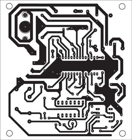
A single side PCB layout for the noise muting FM receiver circuit is shown in Fig. 4 and its component layout in Fig. 5. Provision for a jumper has been made in the PCB so that either a headphone or AF amplifier circuit with speaker may be used as desired.
This PCB can be fitted with a Philips make miniature gang condenser or equivalent for VC1 and VC2. For power ‘on’/‘off’ switch S1 and volume control VR1, a switch-cum-volume control is used in the PCB. The terminals of this switch-cum-volume control need to be directly soldered over the corresponding pads on the PCB.
The article was first published in October 2005 and has recently been updated.

How to change frequency 144 mhz?
I’ve noticed that with the FM muting switch (on the face of my 1978 Pioneer receiver) switched to the ‘On’ position, I hear no hiss when tuning but also no FM signal whatsoever. Even when tuned to an FM station, when I engage the FM muting switch station reception is lost. I do live in a pretty remote location and FM stations are pretty distant to me but I get a small number of stations clear enough to listen to. Except when I engage the FM muting. Then, nothing. Any ideas – anyone?
This circuit is related to FM. Not sure which frequency you are referring to…