


 The need for renewable energy sources is on the rise because of the acute energy crisis in the world today. The main limitation for the saturation and reach of solar PV systems is their low efficiency and high capital cost. In this thesis, we propose a schematic to extract maximum obtainable solar power from a PV module and use the energy for a DC application. This circuit works with the concept of Maximum Power Point Tracking (MPPT) to increase the efficiency of the solar photovoltaic system.
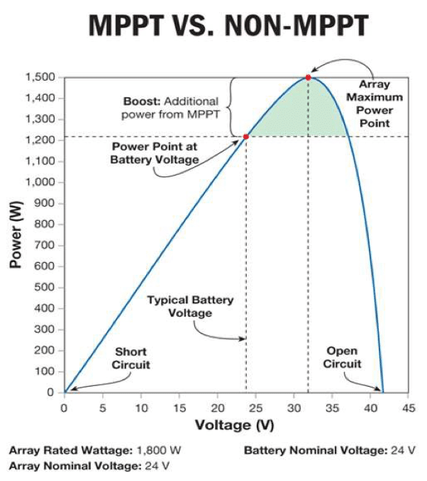
The output power of a PV panel is a function of temperature, radiation and the position of the panel. It is also the function of the product of voltage and current. By varying these parameters, the power can be maximized. To maximize the output power generally, MPPT is used. There are several MPPT method exists in order to maximize the output power. This circuit is based on input voltage-based peak power tracking.
MPPT
A Maximum Power Point Tracker, MPPT, is a high-frequency DC to DC converter. It takes the DC input, from the solar panels in our case, and changes it to high-frequency AC, and then rectifies it back down to a different DC voltage and current to exactly match the panels to the batteries. An MPPT controller “looks” for the point where the sharp peak occurs (below), and then performs a voltage/current conversion to change it to exact values that the battery requires. The peak will always vary due to changes in light conditions and weather.

The application of an MPPT, in the real world, is dependent on the array, climate, and seasonal load pattern. According to Maximum Power Transfer theorem, the power output of a circuit is maximum when the Thevenin impedance of the circuit (source impedance) matches with the load impedance. Hence our problem of tracking the maximum power point reduces to an impedance matching problem. By changing the duty cycle of the boost /buck converter appropriately we can match the source impedance with that of the load impedance.
Project implementation
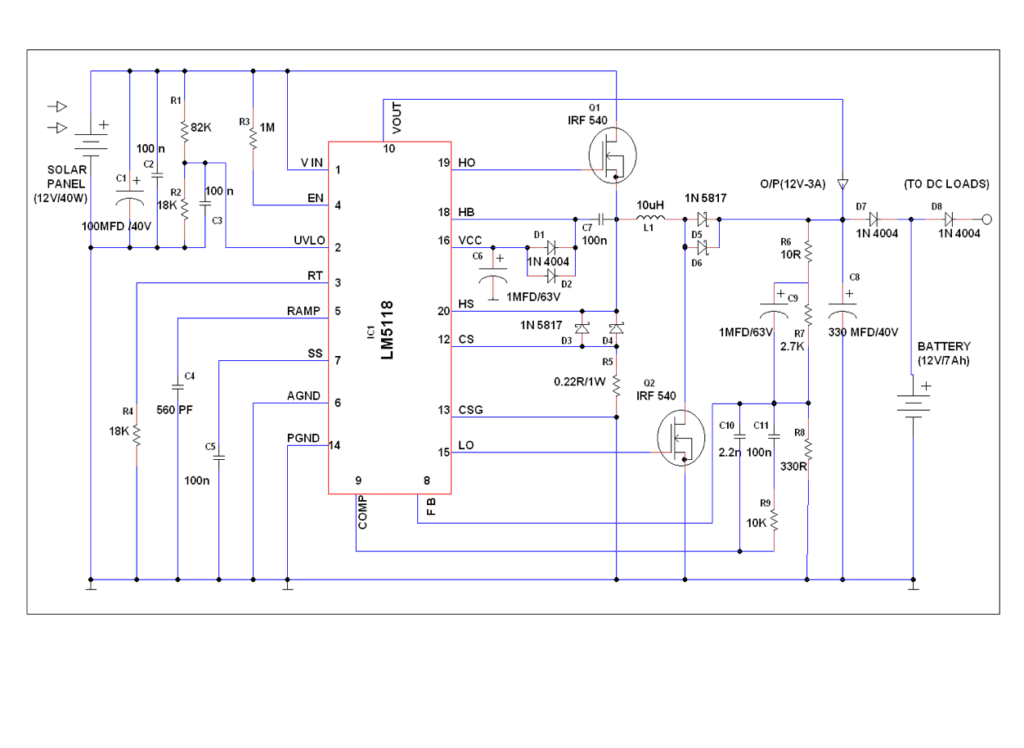
We are going to implement LM5118 IC for maximum power point tracking which features all the functions necessary to implement an efficient high voltage buck or buck-boost regulator using a minimum of external components. The regulator switches smoothly from buck to buck-boost operation as the input voltage approaches the output voltage, allowing operation with the input greater than or less than the output voltage.

This IC integrates high side and low-side MOSFET drivers capable of supplying peak currents of 3 A. The regulator control method is based on output current mode control utilizing an emulated current ramp. The operating frequency is user programmable from 50 kHz to 500 kHz. Fault protection features include current limiting, thermal shutdown and remote shutdown capability.
An under-voltage lockout input allows regulator shutdown when the input voltage is below a user selected threshold, and a low state at the enable pin will put the regulator into an extremely low current shutdown state. These two features can be utilized to make the system in standby mode during night times.
Since the buck-boost power converters are not as efficient as buck regulators, the IC LM5118 has been designed as a dual mode controller whereby the power converter acts as a buck regulator while the input voltage is above the output. As the input voltage approaches the output voltage, a gradual transition to the buck-boost mode occurs. The dual mode approach maintains regulation over a wide range of input voltages, while maintaining the optimal conversion efficiency in the normal buck mode. The gradual transition between modes eliminates disturbances at the output during transitions.
Circuit operation
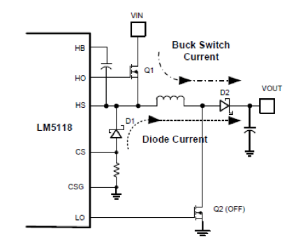
The following figure shows the basic operation of the LM5118 regulator in the buck mode. In buck mode, transistor Q1 is active and Q2 is disabled. The inductor current ramps in proportion to the VIN – VOUT voltage difference when Q1 is active and ramps down through the recirculating diode D1 when Q1 is off. The first order buck mode transfer function is VOUT/VIN = D, where D is the duty cycle of the buck switch, Q1.
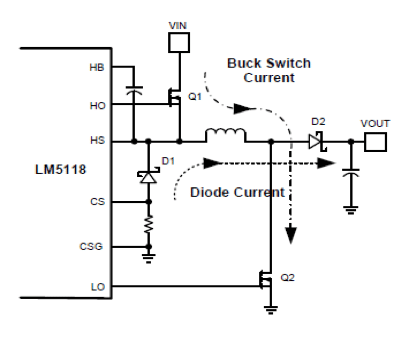
The following figure shows the basic operation of buck-boost mode. In buck-boost mode both Q1 and Q2 are active for the same time interval each cycle. The inductor current ramps up, (proportional to VIN) when Q1 and Q2 are active, and ramps down, through the recirculating diode during the off time. The first order buck-boost transfer function is VOUT/VIN = D/(1-D), where D is the duty cycle of Q1 and Q2.
VIN
The solar panel output is coupled to the V IN pin directly. The capacitors C1 & C2 are used as input filters
UVLO
An under-voltage lockout pin is provided to disable the regulator when the input is below the desired operating range. If the UVLO (pin2) is below 1.13 V, the regulator enters a standby mode with the outputs disabled, but with VCC regulator operating. If the UVLO input exceeds 1.23 V, the regulator will resume normal operation. A voltage divider from the input to ground using R1 & R2 can be used to set a VIN threshold to disable the regulator for low input faults.
Enable
The LM5118 contains an enable function which provides a very low input current shutdown mode. If the EN (pin4) is pulled below 0.5 V, the regulator enters shutdown mode, drawing less than 10 μA from the VIN pin. Raising the EN input above 3 V returns the regulator to normal operation. The EN pin can be tied directly to the VIN pin if this function is not needed. It must not be left floating. A 1 MΩ pull-up resistor to VIN can be used.
Error Amplifier and PWM Comparator
The internal high gain error amplifier generates an error signal proportional to the difference between the regulated output voltage and an internal precision reference (1.23 V). The output of the error amplifier is connected to the COMP pin. Loop compensation components are connected between the COMP and FB (pins 8 & 9). This network creates a low frequency pole, a zero, and a noise reducing high frequency pole. The PWM comparator compares the emulated current sense signal from the RAMP generator to the error amplifier output voltage at the COMP pin. The same error amplifier is used for operation in buck and buck-boost mode.
Ramp Generator
The ramp signal of a pulse-width modulator with current mode control is typically derived directly from the buck switch drain current. This switch current corresponds to the positive slope portion of the inductor current signal. Using this signal for the PWM ramp simplifies the control loop transfer function to a single pole response and provides inherent input voltage feed-forward compensation.
The disadvantage of using the buck switch current signal for PWM control is the large leading-edge spike due to circuit parasitic. The leading-edge spike must be filtered or blanked to avoid early termination of the PWM pulse. Also, the current measurement may introduce significant propagation delays. The filtering, blanking time and propagation delay limit the minimal achievable pulse width. In applications where the input voltage may be relatively large in comparison to the output voltage, controlling a small pulse width is necessary for regulation.
The LM5118 utilizes a unique ramp generator which does not actually measure the buck switch current but instead creates a signal representing or emulating the inductor current. The emulated ramp provides signal to the PWM comparator that is free of leading edge spikes and measurement or filtering delays. The current reconstruction is comprised of two elements, a sample-and hold pedestal level and a ramp capacitor which is charged by a controlled current source as shown in the following Figure.
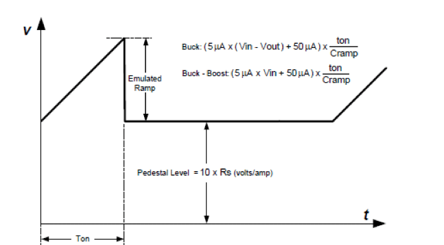
The sample-and-hold pedestal level is derived from a measurement of the recirculating current through a current sense resistor in series with the recirculating diode of the buck regulator stage. A small value current sensing resistor is required between the recirculating diode anode and ground. The CS and CSG (pins 12 & 13) should be Kelvin connected directly to the sense resistor.
The voltage level across the sense resistor is sampled and held just prior to the onset of the next conduction interval of the buck switch. The current sensing and sample-and-hold provide the DC level of the reconstructed current signal. The sample and hold of the recirculating diode current is valid for both buck and buck-boost modes. The positive slope inductor current ramp is emulated by an external capacitor connected from the RAMP (pin5) to the AGND and an internal voltage controlled current source. In buck mode, the ramp current source that emulates the inductor current is a function of the VIN and VOUT voltages
Soft-Start
The soft-start feature allows the regulator to gradually reach the initial steady state operating point, thus reducing start-up stresses and surges. The internal 10 μA soft-start current source gradually charges an external soft-start capacitor connected to the SS (pin 7). The SS pin is connected to the positive input of the internal error amplifier.
The error amplifier controls the pulse-width modulator such that the FB pin approximately equals the SS pin as the SS capacitor is charged. Once the SS pin voltage exceeds the internal 1.23 V reference voltage, the error amp is controlled by the reference instead of the SS pin. The SS pin voltage is clamped by an internal amplifier at a level of 150 mV above the FB pin voltage. This feature provides a soft-start controlled recovery in the event a severe overload pulls the output voltage (and FB pin) well below normal regulation but doesn’t persist for 256 clock cycles.Various sequencing and tracking schemes can be implemented using external circuits that limit or clamp the voltage level of the SS pin. The SS pin acts as a non-inverting input to the error amplifier anytime SS voltage is less than the 1.23 V reference. In the event a fault is detected (over-temperature, VCC under-voltage, hiccup current limit), the soft-start capacitor will be discharged. When the fault condition is no longer present, a new soft-start sequence will begin.
HO Output
The LM5118 contains a high side, high current gate driver and associated high voltage level shift. This gate driver circuit works in conjunction with an internal diode and an external bootstrap capacitor. A 0.1 μF ceramic capacitor, connected with short traces between the HB (pin 18) and HS (pin 20) is recommended for most circuit configurations. The size of the bootstrap capacitor depends on the gate charge of the external FET. During the off time of the buck switch, the HS pin voltage is approximately –0.5 V and the bootstrap capacitor is charged from VCC through the internal bootstrap diode. When operating with a high PWM duty cycle, the buck switch will be forced off each cycle for 400ns to ensure that the bootstrap capacitor is recharged.
Thermal Protection
Internal Thermal Shutdown circuitry is provided to protect the integrated circuit in the event the maximum junction temperature is exceeded. When activated, typically at 165°C, the controller is forced into a low power reset state, disabling the output driver and the bias regulator. This protection is provided to prevent catastrophic failures from accidental device overheating.
A wide operating range of 4 V to 75 V (with a startup requirement of at least 5 V) is achieved using this dual mode regulator. The output of the VCC regulator is current limited to 35 mA, typical. Upon power up, the regulator sources current into the capacitor connected to the VCC pin. When the voltage at the VCC pin exceeds the VCC under voltage threshold of 3.7 V and the UVLO input pin voltage is greater than 1.23 V, the gate driver outputs are enabled, and a soft-start sequence begins. The gate driver outputs remain enabled until VCC falls below 3.5 V or the voltage at the UVLO pin falls below 1.13 V.
For output voltages between 4 V and 15 V, VOUT can be connected directly to VCCX. When the voltage at the VCCX pin is greater than 3.85 V, the internal VCC regulator is disabled and an internal switch connects VCCX to VCC, reducing the internal power dissipation. In high voltage applications extra care should be taken to ensure the VIN pin voltage does not exceed the absolute maximum voltage rating of 76 V.
Hence the buck-boost converter using IC LM5118 is used to speed up responses for reaching the accurate MPPT of solar panel arrays under solar insolation and ambient temperature changes. MPPT controller can fast track the maximum power point, has better response and lower oscillation under rapid atmospheric conditions.

I need urgently IC LM5118 .I am selected the project to work on solar panels mppt using IC LM 5118 for your magazine.
Dear Sir, in the circuit you have shown 12v/7aH battery and the o/p voltage is 12V/3A. But for ideal battery charging for 12v/7ah we require only approx 1A of current then why there is 3A in the circuit.
Hello, this idea for making a buck-boost charger with integrated MPPT sound really interesting.
However it is not clear to me how and where the MPPT action is implemented: wich part of the circuit plays such a role?
Thank you
hi dosent the SLA battery require more than 12v to charge the battery.so in this circuit will it charge the battery..??
hi,
Will SLA battery charge from 12v or does it require more than 12v(14.5v).,
Yes, I have the same thought as Mr Sujit. How this IC perform MPPT?
EFY, can you please test this circuit and confirm if it works perfectly. or provide any other better solution for MPPT Solar charge controller.