




What happens when memory moves closer to the AI processor? A new architecture could reshape how future systems handle data.
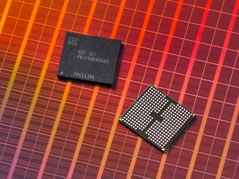
Samsung Electronics showcased memory and storage technologies aimed at addressing the bandwidth, power, latency, and density demands of future artificial intelligence (AI) and high-performance computing systems at Future of Memory and Storage (FMS) 2026 in Santa Clara, California.
The company presented concept models for zHBM and zNAND-O, along with V10 BV-NAND, an architecture using wafer bonding to stack memory cells. The technologies are designed to address growing data movement requirements as AI workloads place greater pressure on memory and storage infrastructure.
The zHBM architecture places high-bandwidth memory directly above an AI accelerator rather than alongside the processor. This shorter data path is intended to increase bandwidth while reducing the energy required for data movement, supporting large-scale AI training and inference.
The architecture also allows customer-specific intellectual property to be integrated between the memory and accelerator. Samsung says a future interface using zHBM could deliver about eight times the performance of HBM5, with wafer bonding enabling more than 10 times its memory density, threefold higher energy efficiency, and more than 50 per cent lower thermal resistance.

The zNAND-O concept is being developed in four- and eight-layer versions for edge AI applications. Based on V-NAND, it combines high storage density with improved I/O performance and low latency for real-time, data-intensive workloads.
V10 BV-NAND uses a new wafer-bonding approach and contains more than 400 layers. The architecture increases memory density by about 58 per cent over the previous V9 generation while improving read, write, and I/O performance.
The wider portfolio included HBM4E samples, HBM5, LPDDR5X-PIM, PM1763, and BM1773 for AI and data-centre applications. “We are developing 3D memory architectures to address the growing performance and efficiency requirements of AI systems,” says Jin-Yub Lee, executive vice president and head of Flash Product & Technology at Samsung Electronics.
Click here for the official announcement.


