


Building AI and 3D chips is getting harder. New design, test, and IP tools aim to reduce complexity and speed development.
Synopsys has expanded its portfolio of AI-powered chip design, verification, testing, and IP solutions for Samsung Foundry’s latest process technologies, helping semiconductor companies develop AI, high-performance computing (HPC), and multi-die chips faster while improving design quality and manufacturing readiness.

The expanded portfolio combines production-ready AI-driven electronic design automation (EDA) tools, certified interface IP, silicon-based signoff technologies, and advanced test solutions optimized for Samsung Foundry’s newest manufacturing nodes. The offerings are designed to address growing chip design complexity, rising development costs, and increasing pressure to reduce time-to-market.
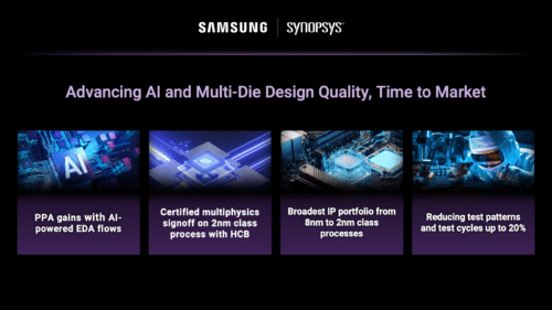
Among the key additions are production-ready AI-powered digital and analog design flows for Samsung Foundry’s third-generation 2nm-class process technology. Through continued design and technology co-optimization (DTCO) efforts between Synopsys and Samsung Foundry, the solutions help customers migrate to advanced nodes while achieving improvements in power, performance, and area (PPA).
Synopsys and Samsung Foundry have also introduced new signoff and analysis capabilities that use silicon feedback to improve design optimization and reliability. These include process sensitivity analysis and power integrity solutions that help engineers make more informed decisions during final verification.
For manufacturing and testing, the companies have expanded AI-assisted design-for-test (DFT) and automatic test pattern generation (ATPG) capabilities. The technologies can reduce test patterns and test cycles by up to 20% while maintaining fault coverage for complex SoCs and multi-die devices. Additional physically aware testing and failure diagnosis features are intended to improve test quality and accelerate failure analysis.
To support next-generation 3D chip architectures, Synopsys and Samsung Foundry are validating a unified exploration-to-signoff platform for Samsung Foundry’s Hybrid Copper Bonding-based 3DIC technology. The platform integrates planning, implementation, and multiphysics analysis in a single environment, enabling optimization across compute, memory, and advanced packaging systems.
The announcement also includes an expanded portfolio of interface, foundation, security, and silicon lifecycle management IP optimized for Samsung Foundry’s advanced and automotive process nodes. The IP is designed to reduce integration risks and support faster product development across AI, HPC, consumer electronics, mobile, and automotive applications.
Click here for the original announcement.
