
ASIP Technologies is building a ₹25 billion semiconductor assembly and test plant in Visakhapatnam, bringing large-scale flip-chip BGA packaging to India.
India’s semiconductor packaging industry is moving from policy plans to physical manufacturing infrastructure. ASIP Technologies, a Hyderabad-based semiconductor company, is developing a 30-acre outsourced semiconductor assembly and test (OSAT) facility at Tarluvada near Visakhapatnam, Andhra Pradesh. The project represents an investment of about ₹2,500 crore and is being developed with South Korean technology partner APACT. According to ASIP, the project represents the first semiconductor packaging partnership of its kind between an Indian and South Korean company.
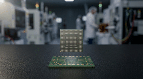
A fabrication plant produces the silicon wafer, while an OSAT facility turns individual dies into packaged components that can be mounted on a circuit board. The process includes thinning and dicing the wafer, attaching individual dies to substrates, forming electrical connections, encapsulating them in mould compound and testing the finished packages. The connection method is particularly important. Conventional wire bonding connects die pads to the package using fine wires, while flip-chip ball grid array (FCBGA) packaging places solder bumps across the die and flips it directly onto the substrate. This provides many more input/output connections with lower electrical inductance, making FCBGA suitable for high-performance processors, graphics processors and networking chips.
ASIP has stated an annual capacity of 96 million chips. The facility will initially support wire-bond and flip-chip BGA packaging, with 2.5D packaging targeted for 2030. ASIP expects the facility to reach production readiness in roughly 18 months, with about 12 months allocated to the cleanroom and building infrastructure, followed by three to four months for equipment installation and trials and around three months for qualification. The company has also begun building its engineering team, with more than 25 engineers hired in Hyderabad and an initial group expected to travel to South Korea for training.
Packaging has not been completely absent from India, but domestic operations have largely remained at smaller scale and focused on legacy wire-bond formats. The country is now building capability in more advanced packaging technologies, including flip-chip BGA and, eventually, interposer-based designs. The supporting supply chain is also developing as companies including Micron, CG Semi and Kaynes work with suppliers to increase domestic sourcing. Against established OSAT markets in Taiwan and China, ASIP’s planned 96-million-unit annual capacity represents an early step in building India’s semiconductor packaging ecosystem rather than a direct challenge to the industry’s largest incumbents.
ASIP is one of nine projects approved under the first phase of the India Semiconductor Mission, which provides a $10 billion government support framework with incentives covering up to 50 per cent of eligible project costs. The other approved projects include Micron, Tata Semiconductor Assembly and Test, CG Semi, Kaynes Semicon, 3D Glass Solutions, Continental Device India, SiCSem and Suchi Semicon. Their packaging strategies vary. CG Semi is developing QFN and thin-shrink small-outline package lines with Renesas Electronics and Stars Microelectronics, while Kaynes is targeting high-power devices rated up to 3300V and 1800A. Kaynes also expects to bring a flip-chip packaging line online next year, followed by a wafer-bumping facility in the first quarter of 2028.
At present, these facilities remain under development, so the production dates cited are targets rather than confirmed operating dates. Qualification will be a key milestone, as packaged devices must meet customer reliability and performance requirements before entering volume production. The initial flip-chip BGA capability is also a mainstream packaging technology rather than the advanced 2.5D packaging used for some high-end AI accelerators. ASIP’s 2.5D and silicon-interposer capability is targeted for 2030, meaning India will continue to depend on overseas advanced-packaging capacity for such applications until that capability is established domestically.
For an Indian design house, the practical benefit would be shorter turnaround times and lower logistics exposure. A fabless startup in Bengaluru or Hyderabad may currently send wafers overseas for assembly and testing before importing the finished devices back to India, adding shipping time, customs procedures and currency exposure to each silicon revision. A qualified FCBGA line in Visakhapatnam could remove one international leg from that process, while the site’s access to the port provides a logistical advantage. ASIP has also partnered with IIT Tirupati on testing and IIT Hyderabad on packaging, helping build the engineering talent needed for domestic assembly and test operations. However, until ASIP’s lines complete customer qualification and meet production quality requirements, the facility remains planned capacity rather than an established alternative in an Indian chipmaker’s supply chain.
For more information, click here.