




Can transistors keep shrinking without losing control? An atomically thin interface offers a possible route beyond conventional silicon scaling.
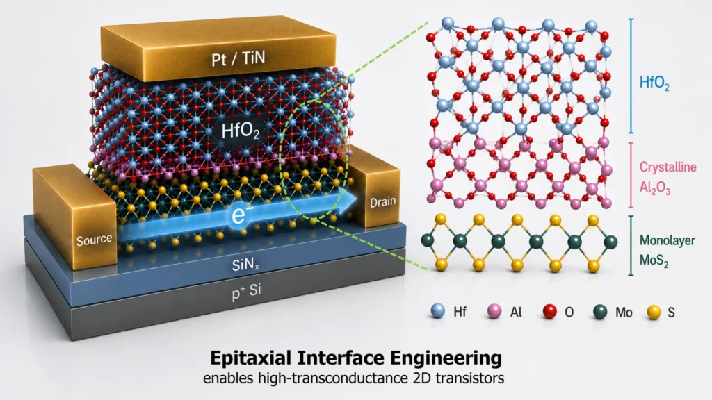
Researchers from TSMC and National Yang Ming Chiao Tung University have demonstrated a transistor interface using a 0.42nm aluminium oxide layer, addressing a key challenge in scaling two-dimensional semiconductor devices. The work centres on molybdenum disulfide (MoS₂), an atomically thin semiconductor being studied for future transistor architectures.
The interface is designed to provide stronger electrostatic control while keeping the insulating layer extremely thin. This is important as conventional approaches face increasing difficulty in maintaining transistor performance when device dimensions approach the sub-nanometre scale.
The resulting device achieved a transconductance of 0.45mS μm⁻¹ with an equivalent oxide thickness of about 1nm. The reported combination indicates that very thin gate interfaces can maintain useful electrical control in MoS₂-based transistors.
The approach could support future devices with thinner channels and shorter gate lengths. MoS₂ has a natural thickness of about 0.7nm, making it suitable for exploring transistor dimensions below those achievable with conventional bulk semiconductor materials.

The researchers formed the interface using epitaxial aluminium deposition followed by controlled oxidation. The process produces an approximately 0.42nm aluminium oxide buffer layer, corresponding to about two atomic layers. The extremely thin interface helps improve electrostatic coupling between the gate and the two-dimensional channel.
However, the technology still faces challenges related to atomic-scale defects and device-to-device variation. Interface states, oxygen vacancies, and other local structural differences can influence leakage and electrical characteristics. Further analysis of the atomic structure and its relationship with device performance will be important for determining whether the approach can be scaled reliably.
The work highlights how controlling interfaces, rather than simply reducing transistor dimensions, is becoming increasingly important at atomic scales.

