As package sizes grow, warpage can become a real headache. A ceramic approach can offer rigidity where traditional materials fall short.
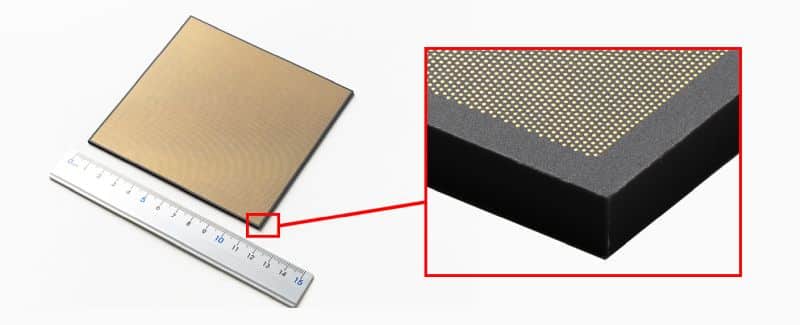
Kyocera Corporation has commercialized a new multilayer ceramic core substrate designed for advanced semiconductor packages such as xPUs and switch ASICs, addressing the rising complexity of AI driven data center architectures. Built using proprietary fine ceramic materials, the substrate is engineered for high density wiring and improved structural rigidity, and will be showcased at ECTC 2026 in Orlando.

The technology aims to improve performance and reliability in large, high integration semiconductor packages. As package sizes increase, conventional organic core substrates often face challenges such as warpage and limitations in wiring density. Kyocera’s ceramic based approach offers higher resistance to deformation, helping maintain structural stability during mounting processes and enabling the use of thinner substrates.
A key benefit of the multilayer ceramic structure is its support for circuit miniaturization. Vias are formed while the ceramic is still pliable, allowing finer diameters and tighter pitch compared to traditional drilling methods used in organic materials. This enables more compact and efficient routing, supporting higher density interconnections required in advanced semiconductor designs.
In terms of applications, the substrate is suited for AI data centers, high performance computing systems, and advanced packaging techniques such as 2.5D integration, where multiple chips are combined on a single interposer to enhance processing capability.

Additionally, Kyocera provides simulation support during the design phase, including thermal, electrical, and warpage analysis. This helps align substrate performance with device level requirements and improves development efficiency for customers.
The company stated it will continue developing packaging technologies to meet evolving semiconductor industry demands.
Click here for the official announcement.