




A doping-free superjunction using gallium nitride’s own polarisation fields lets lateral devices on silicon block nearly four kilovolts, far beyond conventional GaN power devices.
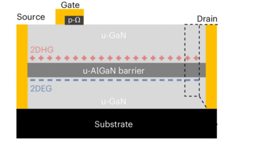
Researchers at the Power and Wide-band-gap Electronics Research Laboratory (POWERlab) at EPFL in Lausanne have demonstrated GaN power devices capable of blocking nearly four kV on a silicon substrate. The devices use what the researchers call an intrinsic polarisation superjunction. A conventional superjunction balances positive and negative charge regions so that the electric field is distributed more evenly instead of concentrating in one region. In silicon, this charge balance is created through carefully controlled doping. GaN can achieve a similar effect using its inherent polarisation fields, eliminating the need for intentional doping in the drift region.
GaN has both spontaneous and piezoelectric polarisation. At a GaN/AlGaN interface, these polarisation fields can create a two-dimensional electron gas (2DEG), while the opposite interface can support a two-dimensional hole gas (2DHG). The EPFL structure combines both in the same epitaxial stack, allowing the positive and negative charge densities to balance each other without intentional doping in the drift region.
The team measured a 2DEG sheet concentration of 1.03 × 10¹³ cm⁻² and a 2DHG concentration of 1.05 × 10¹³ cm⁻², corresponding to a charge mismatch of less than 2 per cent. The epitaxial stack is built on six-inch silicon and consists of a 7-µm buffer, 400-nm undoped GaN channel, 30-nm undoped Al0.35GaN barrier, 300-nm undoped GaN cap and a 50-nm magnesium-doped p-GaN layer used only to form a low-resistance ohmic contact. Yuan Zong, co-first author, explained the importance of avoiding dopants: “Doping-based charge balancing in GaN can be highly temperature sensitive. Our doping-free design is key to the robustness of our device.”
Schottky barrier diodes with a 25-µm superjunction length blocked more than 3.9 kV, with a specific on-resistance of 4.7 milliohm·cm² and a turn-on voltage of 0.75 V. At 125°C, the breakdown voltage remained above 3.3 kV.
The team also demonstrated transistors. The depletion-mode device blocked more than 3.5 kV with a specific on-resistance of 6.3 milliohm·cm² and a threshold voltage of −7 V. The enhancement-mode device blocked more than 3.4 kV, with a specific on-resistance of 11.1 milliohm·cm² and a threshold voltage of 0.67 V. Both transistors achieved an on/off current ratio above five orders of magnitude, showing that the polarisation-based charge-balancing approach can be extended beyond diodes to high-voltage GaN transistor structures.
Commercial GaN power transistors are typically rated around 600–650 V, making the EPFL devices capable of blocking more than five times the voltage of many commercially available GaN transistors. Professor Elison Matioli, who heads POWERlab, highlighted the advantage of using GaN’s inherent polarisation: “We achieve this by exploiting a natural polarization effect that is unique to GaN. Our work could enable robust, efficient, high-voltage power electronics at much more compact scales.”
Dynamic on-resistance provides a more demanding test because trapped charge can temporarily increase a GaN device’s resistance after it has been held at high voltage, increasing switching losses in practical converters. In the team’s measurements, the control Schottky diodes showed dynamic on-resistance increases of more than 50 times their static value at reverse biases as low as 200 V. By comparison, the iPSJ diodes remained within 15 per cent of their static on-resistance up to 3 kV, indicating substantially more stable high-voltage switching behaviour.
These are laboratory devices fabricated on six-inch silicon, and the demonstrated structures are lateral rather than vertical. The authors identify breakdown in the GaN-on-silicon buffer as the current voltage limitation, suggesting that higher blocking voltages could be achieved using sapphire or bulk GaN substrates. The measurement setup also could not characterise the dynamic performance of the transistors above 3 kV, and the study does not report long-term production-scale reliability data.
Luca Mazzone, the other co-first author, highlighted potential applications in high-voltage systems: “Our device can hold high voltage across a wide temperature range, making it suitable for EVs or industrial power systems, where electronics must operate reliably under high temperatures and electrical stress.” Professor Matioli said the group’s next step is to combine the intrinsic polarisation superjunction approach with its earlier work on reducing device resistance.
The important detail for Indian manufacturing is the substrate. This is GaN-on-silicon, grown on six-inch silicon wafers, meaning the technology can potentially use established silicon wafer-processing infrastructure rather than requiring a manufacturing ecosystem based entirely on specialised bulk GaN substrates. That could reduce the manufacturing barrier compared with processes that require dedicated compound-semiconductor substrates.
India’s demand for kilovolt-class power devices spans several areas. High-power EV charging, grid-connected solar inverters, industrial drives and traction systems all require switches capable of handling voltages beyond the range of many commercial GaN devices, with silicon carbide and silicon IGBTs currently filling much of that higher-voltage space. India’s semiconductor programme includes the Modified Scheme for setting up of Compound Semiconductors / Silicon Photonics / Sensors (including MEMS) Fabs / Discrete Semiconductor Fabs and Semiconductor ATMP / OSAT facilities, which provides 50 per cent capital-expenditure support for eligible facilities.
Indian power-electronics companies designing at these voltage levels still rely heavily on imported power semiconductors. A GaN process that demonstrates more than 3 kV blocking on a silicon substrate could therefore expand the range of high-voltage devices that a domestic semiconductor facility could eventually target. The EPFL work remains a laboratory demonstration, not a production-ready process, but its combination of high-voltage GaN, polarisation-based charge balancing and silicon substrates makes the direction particularly relevant to India’s emerging power-semiconductor manufacturing ecosystem.
For more information, click here.

