Focused microwave-based 3D printing enables precise, localised heating of electronic materials, allowing complex, multi-material devices to be fabricated in a single process without damaging surrounding structures.
A new electronics manufacturing technique using focused microwaves is redefining how 3D-printed devices are built, enabling complex, multi-material structures that were previously difficult or impossible to produce.

Researchers led by Rice University have developed a process that integrates targeted microwave heating into 3D printing, solving a long-standing limitation in printed electronics: how to process conductive inks without damaging surrounding materials.
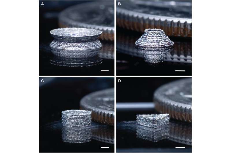
Traditional 3D-printed electronics require heat treatment to activate conductive inks, but that heat often spreads and degrades nearby components, restricting material choices and device complexity. The new approach concentrates microwave energy into a tiny region, about the width of a human hair, allowing selective heating of printed materials while keeping adjacent layers intact.
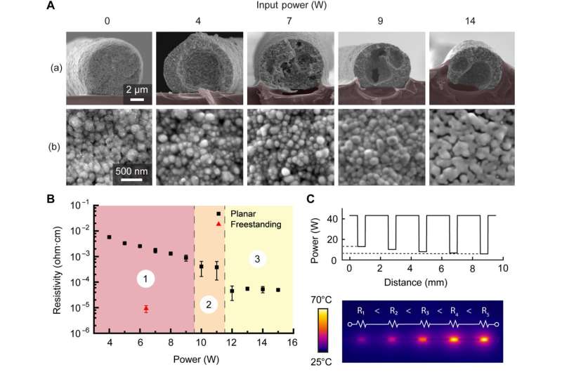
At the core of the system is a device called Meta-NFS (metamaterial-inspired near-field electromagnetic structure), which enables precise control of microwave energy during the printing process. By tuning the microwave parameters, researchers can directly program the electrical and mechanical properties of materials in real time, effectively embedding functionality into the structure as it is printed.
This capability marks a shift from conventional electronics manufacturing, which typically relies on centralised fabrication and multi-step assembly. Instead, the new method enables continuous, desktop-scale production of electronics with integrated functionality, reducing complexity and enabling more flexible designs.
The process is compatible with a wide range of materials, including metals, ceramics, and polymers, and can even be used on temperature-sensitive substrates such as biopolymers and biological tissues. Researchers demonstrated the printing of wireless sensors directly onto objects such as bone and plant leaves, highlighting potential applications in healthcare, bioelectronics, and environmental monitoring.
Beyond prototyping, the technology could support entirely new classes of devices, including ingestible sensors, bionic systems, and soft robotics with embedded electronics. By enabling spatial control over material properties within a single print, focused microwave 3D printing positions itself as a foundational step toward fully integrated, next-generation electronic systems.