Researchers grow magnetic materials on wafer-scale surfaces, moving beyond flakes and enabling use in spin-based devices, sensors, and data storage systems.
Researchers from the Indian Institute of Science have found a way to grow ultra-thin magnetic materials across centimetre-scale wafers, addressing a key limitation that has kept these materials confined to lab experiments.

These materials, known as 2D magnetic materials, are only a few atoms thick but still retain magnetic properties. They are relevant for devices such as hard drives, sensors, and “spintronics” technologies that rely on electron spin rather than charge. Until now, they could only be produced as tiny flakes, which limited their use in real systems.
The team, led by assistant professor Akshay Singh, developed a process to grow these materials over large areas similar to chip wafers. Their work, published in Advanced Materials, replaces the common lab method of peeling thin layers from bulk material with a growth-based approach.
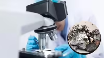
They used Physical Vapour Transport Deposition (PVTD), where the material is vapourised and then deposited as a thin film on a surface. The main challenge was to maintain uniform growth without defects, since small variations can change magnetic behaviour.
To control this, the researchers reduced excess heat and light in the chamber, increased carrier gas flow rates beyond standard levels, and regulated how the material was supplied during growth. They also removed oxygen and moisture to prevent damage.
Surface selection was another factor. After testing different options, synthetic mica allowed the material to form smooth and ordered layers. The team also showed that these films can be transferred onto other surfaces, which is required for device integration.
The same method could be applied to other sensitive materials, which may support future work in electronics and data storage.