


An ultra-fine solder paste boosts print consistency, cuts cleaning time, and delivers reliable reflow performance for next-gen semiconductor packaging.
As the electronic assemblies are shrinking, the architectures grow more complex and the manufacturers face increasing pressure to achieve uniform, repeatable and fine-feature printing. Traditional solder pastes often struggle with aperture sizes below 80μm, leading to inconsistent deposits, voiding, slumping, and frequent stencil cleaning. These issues reduce the overall yield and slow down production.

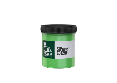
Indium Corporation introduces SiPaste C312HF, a cleanable, halogen-free solder paste formulated with Type 7 powder. It is specifically formulated for printing apertures as small as 60μm. By optimizing both powder morphology and flux chemistry. The paste enables stable transfer efficiency, long stencil life, and reliable reflow behavior for next-generation semiconductor packaging lines.
The paste offers a range of characteristics, which includes:
- Consistent with low standard-deviation deposit volumes
- Excellent slump resistance preventing bridging and defects
- Low voiding across component types
- Optimized powder and flux formulation for fine-feature control
- Minimal stencil cleaning requirements
- Wide reflow profile window compatible with varied processes
- Increased wetting capability across multiple metallizations
- Cleanable post-reflow residue
By delivering reliable fine-feature printing and reducing process interruptions, the paste helps boost yields, minimize rework, and maintain tighter quality control. Its dual cleanability or no-clean flexibility supports diverse production environments, while its performance aligns with industry goals and supports consistent printing performance across advanced packages.
As feature sizes continue to shrink and packaging demands rise, the solder paste enables efficient system-in-package designs and supports next generation electronics manufacturing roadmaps.
