


Atoms in semiconductors do not mix randomly. They form patterns that change how electronics work. Understanding these patterns could open possibilities for future devices.
Designing semiconductors with specific electronic properties is a challenge for engineers working on quantum computing, optoelectronic devices, and defense technologies. A key problem is that trace elements in semiconductor crystals, though present in small amounts, can alter the material’s behavior. Until now, it was unclear how these atoms were arranged locally, making it difficult to predict or control semiconductor performance.

Researchers from Lawrence Berkeley National Laboratory and George Washington University have shown that atoms in semiconductors form localized patterns, rather than mixing randomly. These patterns, known as short-range order (SRO), influence electronic properties such as the band gap, which controls the material’s behavior in microelectronics. The work, published in Science, could guide the design of semiconductors for quantum computing and optoelectronic applications.
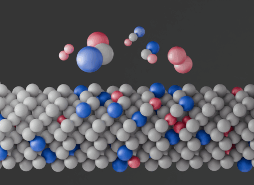
At the atomic level, semiconductors are crystals with repeating lattice structures, usually composed mostly of one element with small amounts of others added. These trace elements are too few to form a repeating pattern across the whole material, and until now, no microscopy or characterization method could detect how they sit next to their neighbors.
The breakthrough came while studying a germanium sample containing small amounts of tin and silicon using a form of electron microscopy called 4D-STEM. Initial results were unclear due to weak signals from the trace elements, but the addition of an energy-filtering device improved contrast and revealed repeating atomic patterns, showing the atoms exhibit local order.
To interpret these patterns, researchers collected data and applied a pre-trained neural network to sort diffraction images. They identified six recurring motifs representing atomic arrangements. To determine the structures behind these motifs, collaborators used a machine-learning potential capable of simulating millions of atoms, performing virtual 4D-STEM on candidate structures until matches were found for the experimental motifs.
This combined experimental and computational approach provided the first direct observation of SRO structural motifs in semiconductors. The study showed that SRO signals, previously difficult to detect due to defects and atomic motion, can be isolated and analyzed using this method.
Follow-up work is exploring how these SRO motifs influence electronic properties, with the goal of manipulating atomic order to enable device functionalities and processing techniques. This research opens the door to designing semiconductors at the atomic scale, allowing control of band structures for applications ranging from topological quantum materials to neuromorphic computing and optical detectors.
