


Tessent Multi-die software solution can help simplify critical design-for-test (DFT) tasks for complex integrated circuits (ICs) based on 2.5D and 3D architectures.
The quest for developing compact and energy-efficient devices has led designers to create more power-efficient and power-dense ICs. These next-generation devices are made possible by employing 2.5D and 3D architectures that connect dies vertically (3D IC) or side-by-side (2.5D) so that they behave as a single device. To simplify the process, Siemens Digital Industries Software has released a new software solution called Tessent Multi-die software solution.

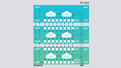
The rapid adoption and deployment of designs featuring densely packed dies in 2.5D and 3D devices have increased the IC test complexity. To tackle this problem the Tessent Multi-die software solution can generate die-to-die interconnect patterns and enable package-level tests using the Boundary Scan Description Language (BS DL). The new software can seamlessly work with other software tools using an integrated Tessent platform, thus reducing test time up to 4X.
According to the company, the Tessent Multi-die software is one of the most comprehensive DFT automation solutions for highly complex DFT tasks associated with 2.5D and 3D IC designs. The software can be used with other software from the Tessent series such as Tessent TestKompress Streaming Scan Network software and Tessent IJTAG software, which optimize DFT test resources for each block without concern for impacts to the rest of the design, thereby streamlining DFT planning and implementation for the 2.5D and 3D IC era. This software enables designers to rapidly generate IEEE 1838-compliant hardware featuring 2.5D and 3D IC architectures.
“As the limits of traditional 2D IC design approaches become increasingly clear over time, more design teams are leveraging the power, performance and form factor advantages that 2.5D and 3D IC architectures can deliver. But deploying these advanced schemes in new design starts without first establishing a DFT strategy that acknowledges the inherent challenges these architectures present can raise costs and undermine aggressive timelines,” said Laurie Balch, president and research director for Pedestal Research. “However, by evolving DFT technology to keep pace with the rapid adoption of multi-dimensional designs, EDA vendors can play a key role in further enabling global, mainstream adoption of 2.5D and 3D architectures.”
Key features
• Dramatically speeds and simplifies critical DFT planning and implementation tasks for next-generation ICs based on 2.5D and 3D architectures
• Enables the rapid generation of IEEE 1838 compliant hardware for 3D IC architectures
• Extracts a single Boundary Scan Description Language (BSDL) for package level and generates patterns
• Extracts die-to-die BSDL and generates boundary-scan-based inter-die patterns
• Supports IEEE 1838 flexible parallel port (FPP) by leveraging the packetized data delivery capabilities of the Tessent Streaming Scan Network (SSN) , which optimize DFT test resources for each block without concern for impacts to the rest of the design
• Ability to adhere and support multiple different standards like IEEE 1687 and IEEE 1149.1
• Seamless integration with other Tessent products using an integrated Tessent platform
