


A chip design tool treats multilayer chips as one 3D structure, reducing wire length by 30% while improving performance and thermal management.
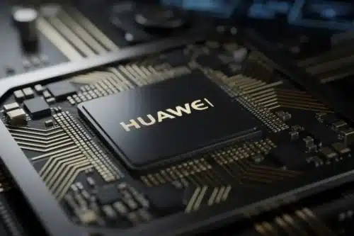
Peking University’s School of Integrated Circuits has developed a prototype electronic design automation (EDA) tool designed for Huawei’s LogicFolding architecture, according to a report by the South China Morning Post. Unlike conventional chip design methods that create each layer separately and then stack them, the new tool treats a multilayer chip as a single three-dimensional structure from the beginning of the design process.

In tests using open-source circuit designs, researchers reported a 30% reduction in total internal wire length compared with traditional EDA workflows. The approach also showed gains in chip performance and thermal management. Huawei aims to achieve transistor densities comparable to 1.4nm process technology by 2031 without relying on extreme ultraviolet (EUV) lithography systems that are subject to U.S. export restrictions.
LogicFolding converts conventional 2D circuit layouts into vertically arranged 3D structures. By shortening the distance electrical signals must travel, the architecture reduces resistance and capacitance in interconnects, helping lower signal delays. Huawei plans to use the technology in its Kirin smartphone processors scheduled for release later this year.
While existing 3D IC design platforms from companies such as Synopsys and Cadence support multi-die integration and advanced packaging, LogicFolding addresses a different challenge. Instead of connecting separate dies or chiplets, it reorganizes transistor-level logic within a single chip into vertical layers. This requires place-and-route tools that can optimize the entire 3D structure simultaneously.
Peking University’s prototype is designed to meet this requirement by treating the full multilayer chip as one unified design space. However, the reported 30% reduction in wire length has so far been demonstrated only on test designs, and its effectiveness in large-scale commercial chip production remains to be proven.
