


Device modeling used to take weeks. Now, AI and automation can do it in hours. See how it makes building models faster and easier.
If you’ve been working on advanced semiconductor designs you know how much more complex device modeling has become. With gate-all-around GAA transistors, wide-bandgap materials like GaN and SiC, and new integration approaches like chiplets and 3D stacking, we’re seeing better performance but also a lot more modeling headaches. Traditional workflows still rely on physics-based compact models and manual tuning which means we have to adjust hundreds of linked parameters across many operating conditions. It’s slow, tricky, and often doesn’t give the best results especially when timelines are tight.
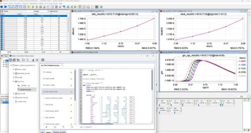
That’s where Keysight’s new Machine Learning Toolkit comes in. It’s part of the latest Device Modeling MBP 2026 suite and it uses neural networks and ML-based optimization to take the pain out of model extraction. With an ML optimizer, auto-extraction flows and supporting utilities, it cuts parameter extraction steps from over 200 to fewer than 10. That means what used to take weeks can now happen in hours.
Key Features and Benefits
- Faster Parameter Extraction: Cuts hundreds of manual steps down to 5–6 automated steps, optimizing 80+ parameters in one run. Captures secondary effects, temperature changes, and dynamic behavior, reducing manual tuning and improving accuracy for DC, RF, and large-signal analysis.
- Automated Workflow: Works directly with Keysight’s Device Modeling platform, supports Python customization, and enables fully automated modeling flows.
- Technology Scalability: Adapts to FinFET, GAA, GaN, SiC, and bipolar devices, providing repeatable and reusable workflows across process nodes.
- Better DTCO Efficiency: Speeds feedback between device and circuit design, cutting PDK development cycles from weeks to days.
Nilesh Kamdar, General Manager of Keysight EDA, said: “AI/ML is fundamentally transforming the traditional workflows and methodologies of compact modeling. With the new Machine Learning Toolkit, we empower our customers to deliver more predictive, higher-quality models in significantly less time — accelerating PDK development and helping them keep pace with rapidly evolving semiconductor technologies.”
