


An undergraduate team is building semiconductor fabrication tools from scratch, showing a practical path to train India’s future chip manufacturing workforce.
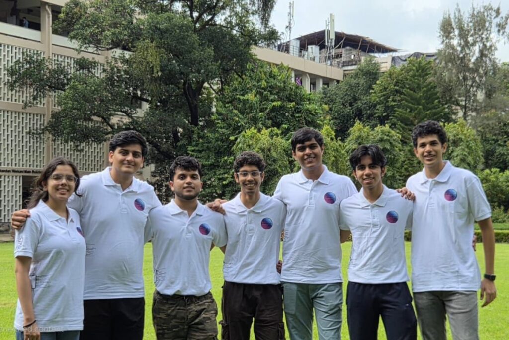
Students at IIT Bombay have built three semiconductor fabrication tools and successfully produced their first silicon devices, demonstrating a low cost approach to training the engineers India urgently needs for its growing semiconductor industry. Operating under the initiative HackerFab IITB, the team expects to fabricate a complete NMOS transistor before the end of the summer.

Founded by Aryamman Bhatia, Abhineet Agarwal and Kartik U C in 2025, the initiative was created to address a critical gap in semiconductor education. While India is investing heavily in new fabrication plants, most engineering students never gain hands-on experience because advanced nanofabrication facilities are reserved for research and are too expensive to use for routine training.
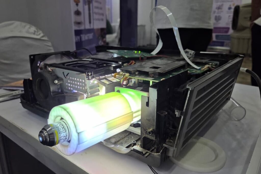
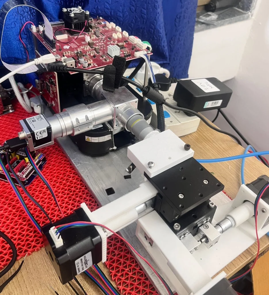
To overcome this challenge, the students designed and built their own fabrication equipment at a fraction of commercial costs. Their setup includes a mask less lithography system capable of producing 3 to 4 micron patterns, a tube furnace that maintains temperatures up to 1100 degrees Celsius within ±5 degrees Celsius, and an in house sputtering system for depositing aluminium films. Earlier this month, the team fabricated and tested a PN junction diode and a MOS capacitor using equipment they assembled themselves.
According to the team, a complete undergraduate fabrication laboratory could be built for far below the cost of conventional research facilities. They are also exploring a “Fab in a Box” concept for colleges and a cloud based fabrication service that would allow students from other institutions to design devices and receive fabricated chips for testing.
The initiative comes as India’s semiconductor sector is expected to require around 30,000 skilled professionals by 2027. “Even if you do spend all the money on the capex, and you get all the joint ventures that you want, if you don’t have the talent to run the fabs, you’re not going to be successful,” says Aryamman Bhatia, Co Founder of HackerFab IITB.
