


A compact multiplexer splits THz signals into three ports with low crosstalk, leveraging quantum cascade lasers and metal-polymer waveguide integration.
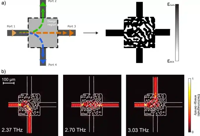
A team of researchers has developed an on-chip active wavelength division multiplexer (WDM) that operates in the terahertz (THz) frequency range, using inverse design and quantum cascade laser (QCL) integration. The device supports three distinct broadband output channels between 2.2 and 3.2 THz and is fabricated on a III–V semiconductor platform using a double-metal waveguide structure.

The multiplexer uses a quantum cascade heterostructure embedded in a metallic cavity, planarised with a benzocyclobutene (BCB) polymer. This approach allows the design to achieve subwavelength dimensions with a footprint of 200 × 200 µm. An inverse design technique, based on gradient-based topology optimisation using SPINS software, was applied to determine the device geometry and permittivity distribution.
The input is fed by an integrated THz QCL frequency comb. Output ports are surface-emitted via broadband patch array antennas. Each antenna handles a specific frequency band, and crosstalk between channels was measured at a maximum of −6 dB. One port (centred at 2.37 THz) showed reduced intensity due to a mismatch between designed and realised spectral ranges.
The WDM section operates independently from the QCL section. It can be biased separately, allowing amplification up to 5.4 dB in selected channels, with saturation observed at 9V. Coherence of the laser output was confirmed using frequency comb measurements and beatnote analysis under injected RF modulation.
Fabrication involved wafer bonding, dry etching, polymer planarisation, and antenna integration. The device was tested in cryogenic conditions and characterised using time-domain and frequency-domain methods, including Fourier transform infrared spectroscopy (FTIR) and SWIFTS.
Applications include compact THz signal routing, coherent THz communications, and integrated spectroscopy. The use of inverse design in this THz implementation demonstrates potential for further integration of gain-enabled components in photonic systems beyond telecom wavelengths.