


Compatible with existing semiconductor processes, this ultra-fast, low-power memory could redefine data storage for AI, edge computing, and future processors.
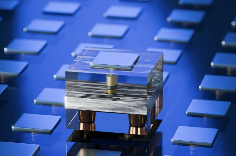
A new tungsten-based spin-orbit torque magnetic random-access memory (SOT-MRAM) could redefine the future of data storage, combining the endurance and speed of DRAM with the non-volatility of Flash—at a fraction of the power cost. Developed by researchers from National Yang Ming Chiao Tung University (NYCU), Taiwan Semiconductor Manufacturing Company (TSMC), and the Industrial Technology Research Institute (ITRI), the device achieves nanosecond-level switching and over 10 years of data retention, according to findings published in Nature Electronics.
The breakthrough centers on tungsten’s exceptional spin-orbit coupling—a property that generates powerful spin currents when an electric charge passes through it. This enables rapid, reliable magnetization switching in the device’s thin ferromagnetic layer, flipping bits in just one nanosecond without external magnetic fields. The result is a fast, non-volatile memory system compatible with existing semiconductor fabrication methods.
Unlike conventional DRAM that requires constant refreshing, or Flash memory that trades endurance for stability, SOT-MRAM offers both. “Our device merges non-volatility with DRAM-level speed but operates at significantly lower power,” said lead researcher Yen-Lin Huang of NYCU. “The key was stabilizing tungsten’s high-efficiency β-phase—typically unstable but essential for strong spin torque—under temperatures up to 700 °C.”
The team demonstrated a 64 kb prototype array, validating its performance under real-world conditions. It achieved switching speeds of ~1 ns and exceptional thermal stability, marking a significant step toward integrating MRAM as on-chip cache or embedded memory in AI accelerators and edge computing systems.
By leveraging industry-compatible processes, the research addresses one of SOT-MRAM’s biggest hurdles: large-scale manufacturability. The ability to produce fast, low-power, and non-volatile memory using existing chip infrastructure could make it a compelling replacement for traditional SRAM and DRAM in next-generation processors.
The group now plans to scale the technology to megabit-class arrays while reducing write energy to sub-picojoule per bit. They are also exploring new oxide and 2D interfaces to enhance efficiency and reliability further. If successful, tungsten-based SOT-MRAM could become the backbone of future AI hardware—where every nanosecond and every milliwatt counts.
