


Ultra-small, low-resistance electrical contacts grown directly on atom-thin semiconductors, marking a critical advance toward sub-nanometer electronics and post-silicon transistor scaling.
Researchers at Nanjing University and other institutes in China have taken a notable step toward ultra-scaled electronics by growing high-performance transistor contacts directly on atom-thin 2D semiconductors, potentially clearing a key bottleneck in next-generation chip miniaturization.
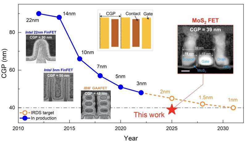
At the heart of the work is a method to form ultra-small, low-resistance electrical contacts on monolayer molybdenum disulfide (MoS₂) , a two-dimensional material with strong prospects as a successor to silicon in nanoscale transistors. The new contacts, made from crystalline antimony, were deposited via molecular beam epitaxy (MBE), a technique that assembles crystals one atom at a time with extreme precision.
What sets this approach apart is how well the resulting contacts scale: resistance remains low even when contact lengths shrink to under 20 nanometers, a range that aligns with targets for the elusive 1 nm logic node. By contrast, contacts created through standard evaporation techniques begin to degrade much earlier as sizes shrink.
Analysts see this as meaningful because contact resistance, not just channel dimensions, increasingly limits transistor performance at atomic scales. Low contact resistance is crucial to maintaining drive currents and efficiency as devices scale down. The work’s extracted transfer length (~13 nm) suggests a path toward practical 2D transistors integrated with future chip architectures.
The researchers demonstrated what could be the smallest high-performance 2D semiconductor transistor to date, underscoring the viability of MoS₂-based electronics as silicon approaches its physical limits. They say the results may help bridge the gap from lab-only demonstrations to real fabrication processes.
Challenges remain, particularly in boosting manufacturability and reliability for mass production and in developing similarly effective p-type contacts, which lag behind their n-type counterparts. Enhancing gate stacks and doping strategies also figures prominently in future work. This advance follows broader industry momentum toward 2D materials as a post-silicon scaling avenue, complementing efforts in integrating 2D layers with silicon chips and improving dielectric/growth processes for ultra-thin devices.