
In an era of electronics based civilisation there is always a demand for more, faster, better and cheaper electronic devices. Electronics started with copper wires and moved to semiconductors (silicon and germanium) base, but now scientists and engineers are putting in efforts to design and develop graphene based electronics for which new applications that fulfil all qualities of desired electronics are emerging very fast. These electronics meet the demands of electronic device-happy and data-centred world of consumers.
Meeting these demands requires technologies for processing and storing information. Now, with the use of graphene, a significant obstacle to the development of next-generation device technologies appears to have been overcome. In simple terms, graphene is a thin layer of pure carbon. It is a single, tightly-packed layer of carbon atoms that are bonded together in a hexagonal honeycomb lattice. Graphene is the world’s first 2D material. Since its isolation in 2004 it has captured the attention of scientists, researchers and industry worldwide with its unique properties.

Some properties of graphene are:
1. It is ultra-light yet immensely tough.
2. It is 200 times stronger than steel, but is incredibly flexible.
3. It is the thinnest material possible and is transparent.
4. It is a superb conductor and can act as a perfect barrier; not even helium can pass through it.

Graphene has been proven to be much more efficient at conducting electrons than silicon, and is also able to transfer electrons at much faster speeds (relatively speaking, 1000 kilometres per second, which is 30 times faster than silicon). In the next few years you will begin to see products from consumer electronics companies using graphene, and electronic devices based on flexible, robust, touchscreen devices such as mobile smartphones and wrist watches.

This could mean foldable televisions and telephones, and eventually electronic flexible newspapers and publications that can be updated via wireless data transfer. Being extremely translucent, in the coming years you can also expect to be able to fit intelligent (and extremely robust) windows in your home, with (potentially) virtual curtains or projected images of your choice.
Soon you will begin to see clothing containing graphene-enhanced photovoltaic cells and super capacitors. So you will be able to charge your mobile telephones and tablet computers in a matter of minutes (even seconds) while walking to work. You may possibly even see security-orientated clothing offering protection against unwanted contact with the use of electrical discharge.
Possibilities of what we can achieve with the materials and knowledge we possess, have been blown wide open. It is now conceivable to imagine such amazing prospective situations as lightning-fast yet super-small computers, invisibility cloaks, smartphones that last weeks between charges and computers that we can fold up and carry in our pockets wherever we go.
The range of applications for graphene in 2D materials in electronics extends far beyond just digital logic. While much research effort is devoted to seeing if graphene can replace silicon as the basis for the next generation of computer chips, this is not its only potential application in the broader field of electronics. In addition to its use in transistors for digital logic, graphene is also being investigated for use in flexible electronics where it can enable conductive inks and serve as a replacement for indium-tin-oxide as transparent conductors in these devices.
There are also the more workhorse roles as an alternative material for interconnects and heat-sinks. Graphene research is focused on applications like energy, membranes, composites and coatings, biomedical, sensors and electronics. This is only the start and these are only the first steps. Potential of graphene is limited only by imagination.
Electronics and energy storage could also be revolutionised by graphene. Flexible, durable, semi-transparent mobile phones, wearable technology, clothing that communicates, electric sports cars and lightweight planes are some of the future technologies that are becoming realistic in our present. Hence, there are a number of growing applications of graphene based technology, but this article is limited to introducing briefly the applications of graphene in electronics.
Graphene based flexible displays
One particular area in which you will soon begin to see graphene used on a commercial scale is in optoelectronics, specifically touchscreens, liquid crystal displays (LCDs) and organic light emitting diodes (OLEDs). For a material to be able to be used in optoelectronic applications, it must be able to transmit more than 90 per cent of light and also offer exceptional electrical conductive properties and therefore low electrical resistance.
Graphene is an almost completely-transparent material and is able to optically transmit up to 97.7 per cent of light. It is also highly conductive and so it would work very well in optoelectronic applications such as LCD touchscreens for smartphones, tablets, desktop computers and televisions.
Researchers have developed a method for producing graphene-treated silver nanowires, which could significantly reduce production costs for nanowire based displays. This could mean that graphene offers a real alternative to indium-tin-oxide in flexible low-cost touchscreen displays. The work has cut the amount of expensive nanowires required to build such touchscreens by more than 50 times besides simplifying the production process by using graphene.
The key to the new process is to exploit graphene’s unmatched conducting properties. To do this, researchers changed from using graphene-oxide that is typically used in a solution based process to create nanowires to pristine graphene. Since pristine graphene is free of oxygen functional groups found in graphene-oxide, it could conduct electricity without any further chemical treatment, which resulted in more than a 50-fold reduction in the number of nanowires needed to produce viable electronic electrodes. This is a real alternative to indium-tin-oxide displays and could replace existing touchscreen technologies in electronic devices.
Energy-efficient transistors
When graphene is placed on top of boron-nitride, it creates a super-lattice, which is a structure made of aligned, alternating layers of various nanomaterials. The super-lattice can move electrons perpendicular to the electric field without the influence of a magnetic field. This could lead to a new kind of energy-efficient transistor. While the research team has not attempted to build a transistor based on the phenomenon, the super-lattice material has displayed high sensitivity to gate voltage that operates transistors.
Another implication of this discovery is that electrons in the super-lattice appear to behave just like neutrinos, which are mass-less particles that do not interact with most kinds of matter. Researchers believe that this discovery could contribute to our understanding of the Universe.
Random access memory (RAM)
Researchers have developed a way of using graphene in order to improve the ferroelectric-tunnel-junction that is a component of RAM. They have improved the ferroelectric-tunnel-junction by combining graphene with ammonia so that it is capable of switching on and off the flow of electrons more completely.
The result is a distinct improvement in the reliability of RAM devices and the ability to read data without having to rewrite it. This is one of the most important differences between previous technology that has already been commercialised and this emergent ferroelectric technology.
In a typical ferroelectric-tunnel-junction design, a ferroelectric layer is placed between two electrodes so that when an electric field is applied to these, direction of the junction’s polarisation is reversed. This reversal of polarisation changes the alignment of positive and negative charges, which correspond to zero and one in binary computing.
Energy storage
Being able to create super-capacitors out of graphene will possibly be the biggest step in electronics engineering. While development of electronic components has been progressing at a very high rate over the last 20 years, power storage solutions such as batteries and capacitors have been the primary limiting factor due to size, power capacity and efficiency (most types of batteries are very inefficient, and capacitors are even less so).
For example, with the development of currently-available lithium-ion batteries, it is difficult to create a balance between energy density and power density. In this situation, it is essentially about compromising one for the other.
Graphene is also being used to boost not only the capacity and charge rate of batteries but also longevity. Currently, while such materials as silicone are able to store large amounts of energy, that potential amount diminishes drastically on every charge or recharge. With graphene tin-oxide being used as an anode in lithium-ion batteries. for example, batteries can be made to last much longer between charges (potential capacity has increased by a factor of ten). And with almost no reduction in storage capacity between charges, it would effectively make electronically-powered vehicles a much more viable transport solution in the future.
This means that batteries (or capacitors) can be developed to last much longer and at higher capacities than previously realised. Also, it means that electronic devices may be able to be charged within seconds, rather than minutes or hours, and have hugely-improved longevity.
Textile electrodes
A team of researchers has used chemical vapour deposition to fabricate monolayer graphene. This research has developed a way to peel graphene off the copper sheet and transfer it to a yarn without compromising the electronic properties of graphene. The methodology that has been developed to prepare transparent and conductive textile fibres by coating these with graphene will now open the way to the integration of electronic devices on these textile fibres.
Researchers envision this process will enable a range of potential applications including textile GPS systems, biomedical monitoring, personal security or even communication tools for those who are sensory impaired.
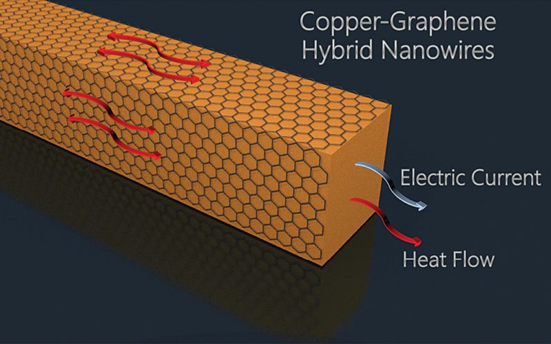
Graphene-coated copper nanowires
In research that sort of bridges flexible displays with interconnects, researchers have been successful in developing copper nanowires coated with graphene to lower resistance and susceptibility to heating of copper wires. This research could allow copper wires to be used in a range of electronics including the flexible variety. Highly-conductive copper nanowires are essential for efficient data transfer and heat conduction in many applications like high-performance semiconductor chips and transparent displays. This is compelling evidence for improved speed and thermal management by adapting the copper-graphene hybrid technology in future silicon chips and flexible electronics applications.
Graphene in thermal management
As circuit densities and clock speeds of chips are steadily rising, thermal-management issues are becoming increasingly paramount. Because of graphene’s high thermal conductivity, it has been investigated as a potential solution to some of these thermal-management issues.
Now, researchers have brought that promise of graphene one step closer with the discovery that, heat propagates in the form of a wave, just like sound in air. This is extremely-valuable information for engineers, who could adapt the design of future electronic components using some of these novel 2D materials’ properties. The work should help engineers better understand the mechanisms of thermal conductivity in graphene and other 2D materials, and become a valuable tool for those who are looking to use graphene for thermal-management solutions.
Magnetised graphene
While the over-riding preoccupation with graphene in electronics may be to see it used in digital logic applications, it may provide enormous improvements to today’s digital memory solutions. Graphene has been imbued with magnetic properties that could lead to a million-fold increase in capacity over today’s hard drives. While some research teams have managed to magnetise graphene, others were able to achieve it with a relatively-simple and scalable process.
Researchers first put a layer of graphene over a silicon wafer. The graphene-covered silicon wafer was then placed into cryogenic ammonia that contained a small amount of lithium. This process adds hydrogen to the wafer, which makes it ferromagnetic. While that is a pretty neat feat, what surprised the researchers was just how evenly the magnetism was spread across the wafer.
The key discovery was that they were able to remove hydrogen atoms from the material using an electron beam. This maintained magnetic areas in some parts of the graphene and removed magnetism from others. This means that large areas of graphene can be patterned with the electron beam to precisely tune magnetism. Since massive patterning with commercial electron beam lithography system is possible, this technique can be readily applicable for current microelectronics fabrication.
Role in spintronics
Spintronics, where the spin of electrons is used to encode information rather than charge, has long promised to be the next step in the evolution of computing. We have already seen evidence of that migration with today’s disk drives that are capable of much greater storage capacities than the previous generation, due to the material phenomenon known as giant magneto resistance.
However, it did not appear as though graphene was going to have much of an impact on the future of spintronics, because if you laid it out flat it did not seem to have any effect on the spin of electrons. This changed when it was discovered that if you put a small bend in graphene it could influence the spin of electrons.
In the latest piece of work, an electron spin has been preserved for an extended distance using large-area graphene. These results would attract a lot of attention in the research community and put graphene on the map for applications in spintronic components.
Paves the way for harmless x-rays. Electromagnetic waves in the terahertz range make it possible to see into the body without using harmful x-rays. Radiation is moderated by water and therefore stops after about a centimetre. But it is precisely its sensitivity to fluids that makes it possible to create an image of various tissues in the body, or to see through clothing, for example. Terahertz radiation requires materials whose electrons can move extremely rapidly, and there are great hopes for graphene.
A team has already constructed a graphene transistor that works at more than ten gigahertz. This research is now proceeding into the terahertz range, which opens up entirely new possibilities. This could lead to soft x-rays for applications in biomedicine or security checks at airports, for instance, where there has been a lack of suitable component materials to deal with sufficiently high frequencies.
Another future scenario is short-distance radars that can penetrate fog and rain up to 100 metres, which might facilitate driving in bad weather.
Technological bottlenecks
The problem that prevented graphene from initially being available for developmental research in commercial uses was that the creation of high-quality graphene was a very expensive and complex process (of chemical vapour disposition). It involved the use of toxic chemicals to grow graphene as a monolayer by exposing platinum, nickel or titanium-carbide to ethylene or benzene at high temperatures.
Also, it was previously impossible to grow graphene layers on a large scale using crystalline epitaxy on anything other than a metallic substrate. This severely limited its use in electronics as it was difficult, at that time, to separate graphene layers from its metallic substrate without damaging the graphene.
However, later studies found that, by analysing graphene’s interfacial adhesive energy, it is possible to effectively separate graphene from the metallic board on which it is grown. Besides, it is also possible to reuse the board for future applications (theoretically, an infinite number of times), thereby reducing the toxic waste previously created by this process.
Further, quality of graphene that was separated by using this method was high enough to create molecular electronic devices successfully. While this research is very highly regarded, quality of graphene produced will still be the limiting factor in technological applications.
Graphene needs to be produced on very thin pieces of metal or other arbitrary surfaces (tens of nanometres thick) using chemical vapour deposition at low temperatures. And it has to be separated in a way that can control such impurities as ripples, doping levels and domain size, while also controlling the number and relative crystallographic orientation of graphene layers. With production techniques becoming more simplified and cost-effective, graphene will be more widely utilised in various applications in general and electronics in particular.
Graphene has a tremendous number of possible applications, and scientists and engineers are just getting started in their work to develop it. Let us hope that their sincere efforts in this direction will create good chances of developing new graphene based electronics applications that are faster, flexible, robust, cheaper and efficient.
Dr S.S. Verma is a professor at Department of Physics, Sant Longowal Institute of Engineering and Technology, Sangrur, Punjab