
It provides a versatile evaluation platform capable of processing input signals from DC to 2 GHz, supporting frequency-domain and time-domain applications.
The Oscilloscope Front-End Reference Design is a versatile and high-performance solution that simplifies the development of precision measurement systems.
Designed to cater to engineers, researchers, and developers, this reference design offers a robust signal acquisition and analysis platform.

The design ensures optimal application performance by featuring key elements such as high-speed analogue-to-digital converters (ADCs), low-noise pre-amplifiers, and configurable signal conditioning circuits.
Ideal for use in electronic test equipment, signal processing labs, and embedded systems development, this design serves as a reliable foundation for creating custom oscilloscope solutions or integrating oscilloscope functionalities into broader systems.
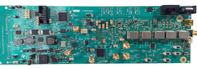
This reference design outlines a high-performance analog front-end tailored for a 50Ω-input oscilloscope application.
The signal chain is designed to ensure optimal signal integrity, precision, and adaptability, making it suitable for advanced measurement and data acquisition systems.
The reference design TIDA-00826 by Texas Instruments, begins with a three-step differential π-attenuator relay circuit for input voltage amplitude adjustment, offering three selectable attenuation settings: 1:1, 2:1, and 5:1.
This is followed by the LMH5401, a low-noise, wideband, fully-differential amplifier (FDA) used for single-ended to differential signal conversion.
It features a 6 GHz bandwidth, excellent linearity from DC to 2 GHz, and low input-voltage noise of 1.25 nV/√Hz, making it ideal for precision signal conditioning.
The LMH6401 digitally-controlled variable-gain amplifier (DVGA) is employed for precise gain adjustment, programmable via an SPI interface in 1-dB steps across a 32-dB range (-6 dB to 26 dB).
This device drives a fifth-order 2.2 GHz low-pass filter, ensuring signal integrity before digitization. An ADC12J4000 12-bit analog-to-digital converter (ADC), operating at 4 GSPS, digitizes the filtered signal.
The ADC boasts excellent noise and linearity performance up to and beyond 3 GHz, achieving an effective number of bits (ENOB) of 6 to 8 for oscilloscope applications.
The design supports AC/DC input coupling with DC offset nulling via a potentiometer. The LMH6559 buffer provides DC-level shift, while an OPA376 servo-loop maintains the ADC’s optimal common-mode voltage.
A 4 GHz ADC clock is generated using the TRF3765 PLL and 100 MHz oscillator, ensuring low phase noise (-128 dBc/Hz at 1 MHz).
The LMK04828 synchronizes the ADC and FPGA for seamless JESD204 communication. With a 2 GHz input bandwidth, ±3V signal support, and +5V or +12V power options, it suits digital oscilloscopes, TDRs, and high-speed data acquisition systems.
TI has tested this reference design. It comes with a bill of materials (BOM), schematics, assembly drawing, printed circuit board (PCB) layout, and more. The company’s website has additional data about the reference design.