As 3D NAND stacks climb past 300 layers, virtual testing reveals how internal stress leads to bending and collapse in memory structures.
As 3D NAND memory devices grow taller, approaching 300 layers, the manufacturers face growing risks of structural failure. A recent simulation-led study using the SEMulator3D platform shows that carefully balancing stress and strain between silicon nitride (SiN) and oxide layers is critical to improving yield and avoiding tier collapse.

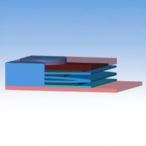
3D NAND relies on vertically stacking alternating metal and oxide layers to boost memory density. But adding more layers introduces mechanical stress, especially in deep layers. One key failure mode is tier collapse, which occurs when oxide cantilevers formed after SiN are removed, leading to bending or breaking of the whole NAND layers during the metal replacement process.
To investigate this, engineers ran two virtual Design of Experiment (DOE) studies using SEMulator3D’s stress analysis tools. They tested how changes in Young’s Modulus, intrinsic stress, material thickness, and cantilever length affect deformation.
Results showed that higher Young’s Modulus values in SiN led to increased displacement and void formation. When the cantilever extended to 700 nm, typical for 300-layer stacks, the stress-induced collapse was observed, particularly when SiN stiffness exceeded 125 GPa(Gigapascals). Oxide thickness also played a role, with thicker oxide reducing deformation.

The second study confirmed that compressive SiN causes more displacement than tensile variants. Matching and reducing the mechanical properties of SiN and oxide, particularly in deeper layers, was found to be most effective in improving structural reliability.
Beyond preventing yield loss, the simulation approach offers an efficient alternative to trial-and-error on real wafers. Engineers can test new layer combinations and structural designs without the time and cost of fab experiments.