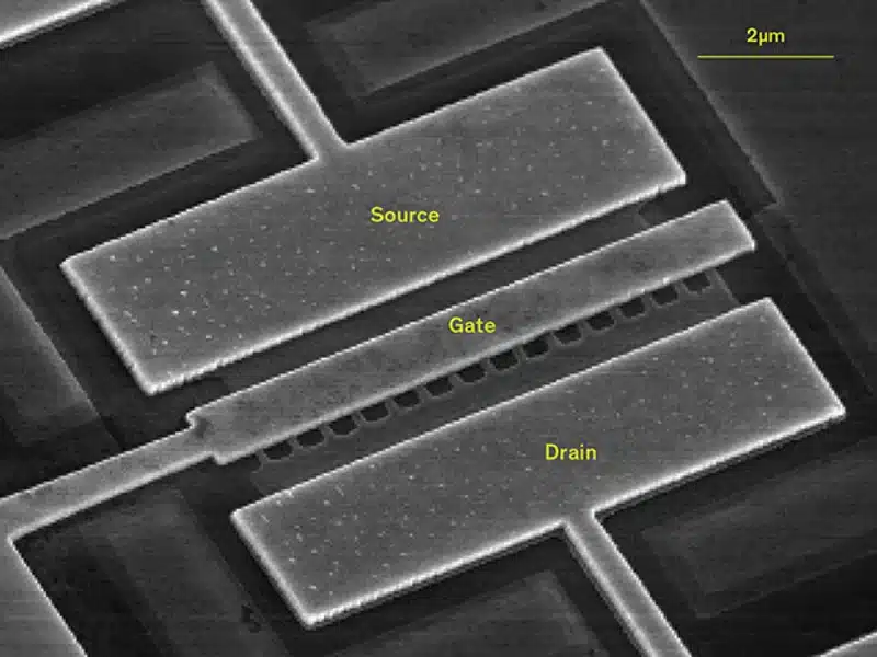
TFETs utilise quantum tunnelling to reduce power consumption and enhance switching speed, offering potential for IoT, neuromorphic, and wearable electronics.

Tunnel field-effect transistors (TFETs) are being developed as a possible alternative to MOSFETs in low-power electronics. MOSFETs use heat to move electrons over a barrier, a process known as thermionic emission. This method has a physical switching speed limit of 60 millivolts per decade at room temperature. Operating at lower voltages leads to leakage, while raising the voltage increases power use.
TFETs work differently, using quantum tunnelling. The gate voltage lines up the energy bands so electrons can pass directly from the source to the channel without needing extra heat. This allows faster switching at lower voltages and reduces leakage, cutting both active and standby power consumption.
These properties make TFETs attractive for applications such as Internet of Things devices, wearable technology, and neuromorphic computing, where low energy use and long battery life are essential. TFETs also handle short-channel effects better than MOSFETs, supporting continued chip miniaturisation.
Material selection is critical to TFET performance. Compounds like indium arsenide and gallium antimonide have low band gaps and light electron mass, improving tunnelling efficiency. Two-dimensional materials such as molybdenum disulfide and tungsten diselenide offer strong control of the channel in compact devices. Designs using layered materials like graphene and hexagonal boron nitride have also shown promise in sensitive electronic applications.
Manufacturing remains a challenge. TFETs require precise band alignment, accurate doping, and defect-free interfaces. Small variations during fabrication can cause significant changes in performance. Work is underway to refine material quality, improve junction control, and adapt processing methods to existing semiconductor production lines.


