Instead of cooling the chip’s surface, the light targets the exact spot inside the chip, where it converts heat into light, increasing performance.
In modern chips, not all transistors are actively used, as it would create hot spots: high temperatures concentrated in tiny areas, reducing overall performance and increasing energy use. This limitation is known as dark silicon.
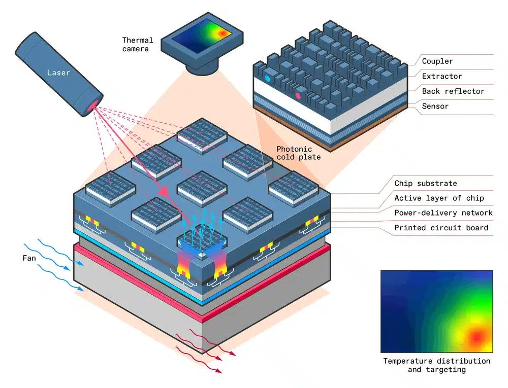
The traditional cooling method removes heat from the chip’s surface, not directly from the inside, limiting how much computing power can be used at once.
A new research approach uses a method called photonic cooling, which turns heat directly into light. The process is based on a phenomenon known as anti-Stokes fluorescence, in which certain materials absorb low-energy laser light and emit higher-energy light.
The additional energy for this light comes from the heat inside the material itself: the heat is converted to light, cooling the chip from inside and directly cooling the transistors during operations.
To apply this concept to chips, a thin photonic cold plate is placed above the chip. Sensors detect where the chip is heating up, and a laser shines on that specific spot. The light interacts with the material in the cold plate, converting heat into light that escapes through an optical layer.
A reflective layer blocks light from re-entering the chip, ensuring the process cools rather than heats. Because the laser can move precisely, it can target and cool hot spots as they form, instead of cooling the entire chip at once.
Early experiments show that photonic cooling can remove more heat than existing air or liquid systems while using less power. This would increase processing speed, reduce energy consumption, and make data centres more efficient by recycling waste heat as usable light energy.