


A three-layer cooler etched in silicon pulls heat from dense chips while using little power, hinting that heat may no longer limit device size.
As electronic devices get smaller and more powerful, they release more heat in less volume. This higher heat density pushes device temperatures up and can damage internal parts over time. That heat is now a limiting factor for compact electronics used in computing, communication, defense, and consumer hardware.

To keep devices safe, engineers use thermal management systems. One approach that is considered promising for compact chips is microfluidic cooling, where fluid is pushed through microscopic channels near or within an integrated circuit so that heat can be carried away. But many earlier microfluidic designs either fail to remove enough heat at high power density or require high pumping power.
Researchers at Peking University and the National Key Laboratory of Advanced Micro and Nano Manufacture Technology have reported a new microfluidic cooling method that can remove heat more effectively and with less power than many earlier strategies. The work, published in Nature Electronics, describes a three-layer cooling device etched directly into a silicon substrate.
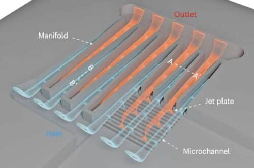
The top layer is a tapered manifold that spreads water across the surface of a chip and ensures that each microchannel receives the same amount of coolant, creating uniform cooling. The middle layer is the microjet layer, which has tiny nozzles that send high-speed fluid streams directly toward the chip surface to break the thermal boundary where heat accumulates. The bottom layer is a microchannel layer with sawtooth-shaped sidewalls that carries the heated coolant away.

The three layers are fabricated using standard MEMS processes on the backside of the silicon. In experiments, the system reached a coefficient of performance of 13,000 and removed a heat flux of 1,000 W/cm² with a maximum temperature rise of 65 K. It also required only 0.9 W/cm² of pumping power and can be manufactured at scale using existing methods.
This work by the Peking University team shows a path to smaller, durable, and energy-efficient electronics by embedding heat removal structures directly into silicon. The design can be refined further and tested across a broader class of compact devices in future studies.
