


An open-source design tool that models how semiconductor components degrade under long-term radiation, giving engineers especially smaller teams new capability to build more reliable electronics for space, medical imaging, and other high-radiation environments.
Space electronics, satellite communications, and even medical imaging systems face a common, often underestimated threat: radiation-induced faults. From cosmic rays hitting satellite processors to high-energy X-rays inside CT scanners, modern electronics are constantly exposed to stress that can trigger memory errors, temporary malfunctions, or long-term device aging. As satellites operate for decades and medical systems demand high reliability, engineers are under pressure to design semiconductor circuits that can survive years of radiation exposure without degrading.
A new research effort from Fraunhofer IIS aims to make this process more accessible and more precise. The institute, working with partners under the FlowSpace project, is developing an open-source tool that models how semiconductor components behave and age under radiation. The goal: give chip designers, especially smaller firms and academic teams, deeper insight into component limits so they can build more resilient circuits without relying on proprietary data they often cannot access.
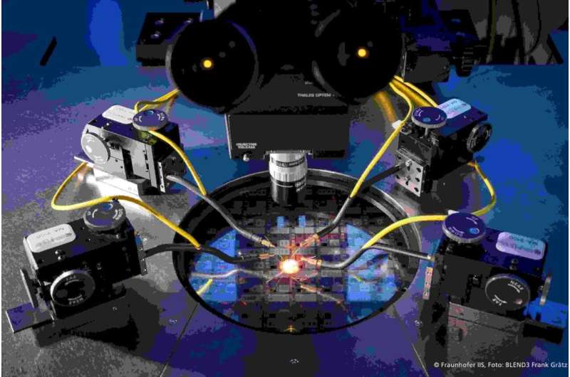
At the core of the initiative is an open process design kit (PDK), positioned as a bridge between semiconductor technologists and chip designers. With openly available device characteristics, design teams can simulate how transistors, interconnects, and other structures will respond to long-term radiation bombardment. This advanced visibility allows them to factor in component aging directly during circuit design, something typically possible only for large semiconductor companies with in-house models. Researchers are validating the system through extensive laboratory simulations, mathematically modeling how specific components degrade when subjected to radiation over a simulated 10-year period. These insights help designers identify failure-prone blocks early and build in targeted redundancy.
The approach is particularly timely as chips continue to shrink. Advanced semiconductor nodes are more energy-efficient and space-saving advantages for aerospace applications but also far more sensitive to radiation. Traditional redundancy strategies often increase die area, but the tool is designed to help optimize these protections, allowing developers to achieve the same reliability with less silicon overhead. By democratizing access to radiation-aware design tools, the Flow Space project could broaden participation in space-grade and medical-grade electronics development, boosting innovation while reducing the barrier to entry for next-generation semiconductor research.
