A new 200-V power MOSFET with ultra-low resistance and advanced topside-cooled packaging enables designers to cut losses, shrink layouts, and reduce the need for parallel devices in high-current industrial and energy systems.
A new high-current power MOSFET by Littelfuse targeting compact, power-dense systems has been introduced to address thermal complexity and component sprawl in modern energy and industrial designs. The device combines a 200-V rating with a current capability of up to 480 A, enabling designers to replace multiple paralleled MOSFETs with a single high-performance switch.

The key features are:
- 200 V rating with up to 480 A continuous current capability
- Ultra-low on-state resistance of 1.99 mΩ
- Topside-cooled, isolated ceramic package for easier thermal design
- Very low junction-to-case thermal resistance of 0.14 °C/W
- Reduced gate charge (535 nC) for improved switching efficiency
At the core of the device is an ultra-junction architecture, this significantly cuts conduction losses in low- to medium-voltage applications where efficiency and heat dissipation are critical design constraints. By reducing both losses and part count, the MOSFET simplifies layout, gate-drive design, and overall system reliability.
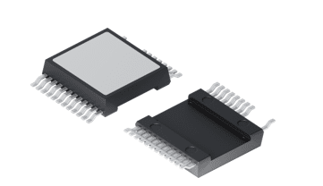
A key differentiator is its ceramic-based, isolated SMPD-X package with topside cooling. The package offers 2.5-kV isolation and a junction-to-case thermal resistance of just 0.14 °C/W, allowing heat to be extracted more efficiently than conventional bottom-cooled power packages. This approach eases thermal design, especially in tightly packed power stages used in energy storage, industrial charging, and high-current DC switching.

The MOSFET’s high current rating allows consolidation of parallel devices that are often required to meet performance targets in battery energy storage systems, industrial power supplies, and charging infrastructure. Fewer parallel switches translate into reduced PCB area, lower assembly complexity, and improved current sharing without elaborate layout techniques. A relatively low gate charge of 535 nC further reduces gate-drive losses, supporting higher switching efficiency at scale.
Target applications include DC load switches, battery energy storage systems, industrial and process power supplies, fast-charging infrastructure, and emerging aerial platforms such as drones and vertical take-off and landing (VTOL) systems, where power density and thermal reliability are tightly constrained. As power electronics move toward higher currents within smaller footprints, devices that combine ultra-low resistance with advanced packaging are becoming essential building blocks. By pairing high current capability with topside cooling and isolation, this MOSFET addresses a growing need for simpler, more robust power architectures across industrial and energy markets.