


A cleanroom-free electronic skin manufacturing process using UV lasers and 3D printing, enabling large-area flexible sensors for robots, wearables, and next-generation human-machine interfaces.
A team of South Korean researchers has unveiled a new fabrication technology that could significantly accelerate the adoption of electronic skin in robotics, wearable electronics and human-machine interfaces. The breakthrough enables large-area flexible sensors to be manufactured directly at the point of use without requiring expensive cleanroom facilities or conventional semiconductor processing infrastructure.
Developed by the Electronics and Telecommunications Research Institute (ETRI) in collaboration with Korea University’s Sejong Campus, the technology replaces traditional semiconductor fabrication steps with a maskless, in-situ manufacturing process. Instead of relying on photomasks, vacuum deposition equipment and etching systems, the approach uses a combination of UV laser processing and 3D printing to create multimodal electronic skin sensors directly on target surfaces.
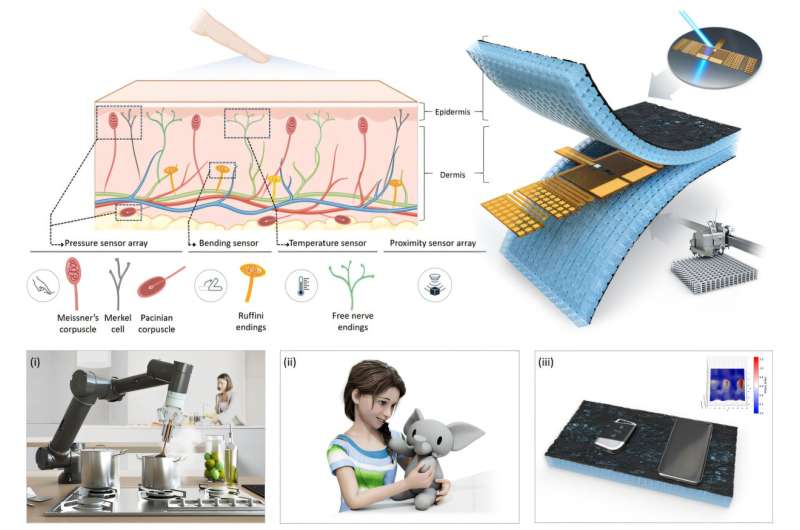
Electronic skin, often referred to as e-skin, is a flexible sensing layer designed to mimic the tactile capabilities of human skin. It can detect pressure, touch and physical interaction, making it a critical technology for intelligent robots that need advanced sensory feedback. However, existing manufacturing methods remain costly and complex because they require controlled cleanroom environments and multiple processing stages. These challenges become even more pronounced when fabricating sensors for large surfaces or irregularly shaped structures.
The newly developed process addresses these limitations by enabling sensor fabrication in a single continuous workflow. Researchers demonstrated a large-area capacitive tactile sensor array built around a microporous dielectric structure, achieving high reproducibility while reducing manufacturing complexity. The elimination of photomasks and transfer steps not only lowers production costs but also improves scalability for commercial deployment.
A key advantage of the technology is its ability to create sensors directly on curved and complex surfaces. This capability is particularly important for humanoid robots, where tactile sensors must conform to arms, hands and other non-flat geometries. The method also supports rapid prototyping, allowing developers to quickly customize sensor designs for specific applications.
Beyond robotics, the technology could enable new classes of wearable health devices, IoT systems and interactive interfaces that require flexible sensing capabilities. ETRI has already demonstrated system-level implementations, suggesting the technology is moving beyond laboratory experimentation toward practical deployment. If commercialized successfully, the innovation could reduce manufacturing barriers and accelerate the development of tactile sensing systems that bring machines closer to human-like interaction capabilities.