


Many electronic circuits require a voltage higher than that available from the power supply. For example, when only a 12V battery or adaptor is available but a circuit requires 20V to 24V, a voltage-boosting arrangement becomes necessary. One simple and economical solution is a charge-pump voltage doubler driven by an oscillator.
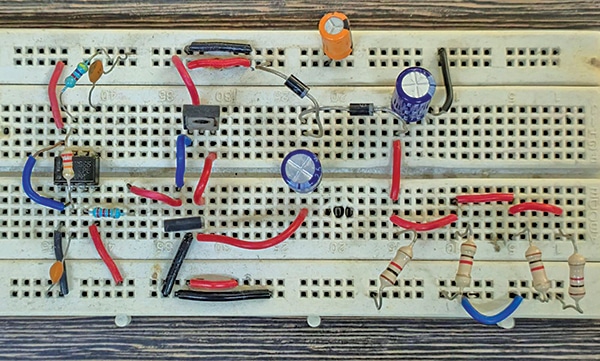
The system is suitable for small power supplies, op-amp circuits, analogue electronics experiments, and various DIY applications that require a moderately higher DC voltage from a lower-voltage source. Fig. 1 shows the author’s prototype.
Circuit and working
Fig. 2 shows the circuit diagram of the voltage doubler system. It is built around the NE555 timer (IC1), transistors BD139 (T1) and BD140 (T2), and a few passive components. The system consists of four main sections: the oscillator stage, the driver stage, the voltage-doubler network, and the output filter stage.
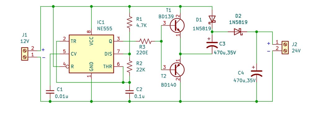
IC1 (NE555) is configured as an astable multivibrator to generate a square-wave signal. Resistors R1 (4.7kΩ) and R2 (22kΩ), together with capacitor C2 (0.1µF), set the oscillation frequency to approximately 3kHz. Capacitor C1 (0.01µF) is connected to the control-voltage pin to improve stability and reduce noise.
The square-wave signal at pin 3 drives the complementary transistor pair comprising T1 (BD139) and T2 (BD140), operating in push-pull mode. This stage improves current-handling capability and enhances the charging and discharging process required for efficient voltage doubling.
The voltage-doubler section is formed by Schottky diodes D1 and D2 (both 1N5819), along with capacitors C3 and C4. During one half-cycle of the oscillator output, capacitor C3 charges through diode D1. During the opposite half-cycle, the stored charge in C3 is added to the supply voltage and transferred through diode D2 to capacitor C4. This action produces an output voltage approximately twice the input voltage.
Schottky diodes are selected because of their low forward-voltage drop and fast-switching characteristics, which improve system efficiency. Capacitor C4 acts as the output filter capacitor, smoothing the pulsating waveform to provide a relatively stable DC output at connector J2.
With a 12V DC supply connected at J1, the system typically produces 20V to 24V DC, depending on the load and component tolerances.
| Parts List |
| Semiconductors: IC1 – NE555 timer IC T1 – BD139 NPN transistor T2 – BD140 NPN transistor D1, D2 – 1N5819 Schottky diode Resistors (all 1/4-watt, ±5% carbon): R1 – 4.7kΩ R2 – 22kΩ R3 – 220Ω Capacitors: C1 – 0.01µF ceramic capacitor C2 – 0.1µF ceramic capacitor C3, C4 – 470µF, 35V electrolytic capacitor Miscellaneous: J1, J2 – 2-pin terminal connector – General-purpose PCB – Suitable enclosure – IC base for NE555 (optional) |
Construction and testing
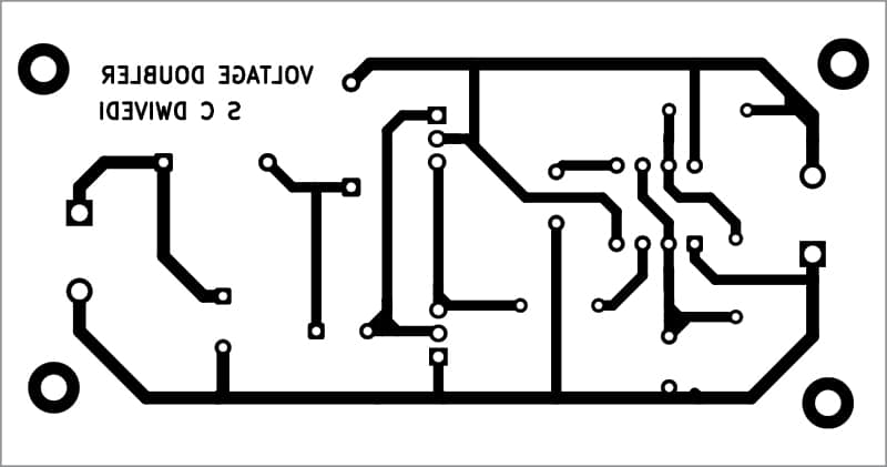
An actual-size single-sided PCB layout for the voltage doubler system is shown in Fig. 3, while the corresponding component layout is shown in Fig. 4. After assembling the system on the PCB, mount it inside a suitable enclosure for reliable operation and protection.
Alternatively, the system may be assembled on a general-purpose PCB or a small perforated board. Begin the assembly by mounting the IC socket for the NE555 timer, followed by resistors R1 and R2, and capacitors C1 and C2 associated with the oscillator section. Ensure proper soldering and correct component placement for stable oscillator operation.
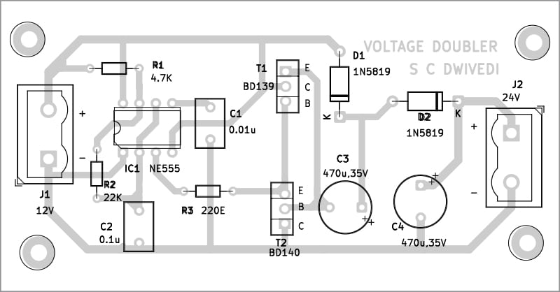
Next, mount transistors BD139 (T1) and BD140 (T2), ensuring the correct orientation of their collector, base, and emitter terminals. For applications requiring higher output current, small heat-sinks may be fixed to the transistors to improve heat dissipation and prevent overheating.
After completing the driver stage, solder Schottky diodes D1 and D2, taking care to observe their polarity. Then solder electrolytic capacitors C3 and C4 with the correct polarity. Finally, connect input connector J1 for the 12V DC supply and output connector J2 for the boosted DC output.
Once assembly is complete, thoroughly inspect the PCB for solder bridges, dry joints, incorrect wiring, or reversed component polarity before applying power.
For testing, connect a regulated 12V DC supply to connector J1. Using a digital multimeter, measure the voltage across output connector J2. Under no-load or light-load conditions, the system should produce an output voltage of approximately 20V to 24V DC.
EFY note. This circuit also operates with lower input voltages. For example, a 6V input can produce approximately 12V, a 9V input can generate around 17V, and a 12V input can deliver nearly 24V. The actual output voltage may vary depending on the load current, input supply conditions, and component tolerances.
Bonus. You can watch the video of the tutorial of this DIY project at
S.C. Dwivedi is an electronics enthusiast and circuit designer at EFY