


Wafer-scale fabrication of heat-resistant transistors could enable integrated circuits for extreme environments, supporting future sensing, aerospace, geothermal, and planetary exploration applications under demanding thermal conditions.
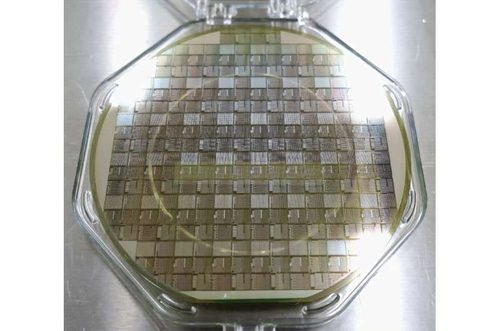
Kyoto University researchers, in collaboration with Phenitec Semiconductor Corp, have successfully fabricated silicon carbide (SiC) junction field-effect transistors (JFETs) on six-inch wafers, advancing the technology towards integrated circuits capable of operating in extreme environments. The wafer-scale devices demonstrated high uniformity, with threshold-voltage standard deviation below 0.07V in the wafer centre.
The work builds on an earlier SiC JFET structure demonstrated by the research team for operation at temperatures up to 600°C. The earlier design used a bottom-gate structure and well-based isolation to improve threshold-voltage control and suppress leakage currents at elevated temperatures.
Moving from individual devices to wafer-scale fabrication is important for developing integrated circuits because practical ICs require large numbers of small, consistently manufactured transistors. The researchers transferred much of their existing JFET fabrication process to Phenitec’s mass-production facility while accounting for industry-standard manufacturing requirements. The process was transferred without major obstacles.
The resulting six-inch SiC wafer demonstrated high device uniformity, with the threshold-voltage variation remaining particularly low across its centre region. This establishes a manufacturing pathway for producing multiple transistors together rather than relying solely on laboratory-scale fabrication.
SiC’s ability to withstand high temperatures makes it attractive for electronic systems exposed to conditions beyond the operating range of conventional silicon devices. Potential applications include jet-engine sensors, geothermal equipment and planetary exploration systems, where electronics must continue functioning under severe thermal conditions.
The researchers now plan to develop more complex circuits and address packaging requirements for extreme environments. The team is also pursuing industry-academia collaboration towards establishing a startup, although the technology remains at the research and development stage rather than being a commercial semiconductor product.