
Clear solar cells in greenhouse roofs could generate electricity while plants grow below.
Because the visible and the infrared (IR) regions of light take up about 47 and 51 per cent of energy in the solar spectrum, respectively, utilising visible light for plant growth and IR light for power generation is extremely exciting. Fig. 1 shows such a concept. IR-absorbing transparent organic photovoltaics (TOPV), with localised IR absorption and visible light transmittance, would be promising materials for this purpose.
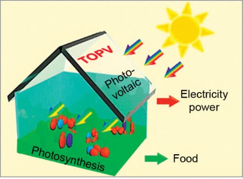
These TOPV would also be flexible enough to be spread easily over contours of a greenhouse roof. Using solar cells for both power generation and farming is a clever idea. In the near future, greenhouses might become more popular for farming. As climate change makes growing conditions less predictable, greenhouses could give farmers more control.
Guidelines for selecting solar cells
While implementing this idea commercially, certain factors must be taken into consideration. Solar cells are devices that turn sunlight into electricity. This technology offers a more Earth-friendly way to produce power than burning coal and other fossil fuels. But panels of solar cells need a lot of open, sunny spaces to harvest that sunlight. Where space is limited, people might have to choose between solar panels and fields to grow food. But what if they want to produce crops and electricity at the same time?
The solution is installation of clear solar cells. However, whether enough light can pass through solar cells is not the only factor an engineer needs to think about; there is also efficiency. Common rooftop silicon solar cells, which absorb visible light, have an efficiency of about eighteen per cent. This means, these produce eighteen watts for every hundred watts of sunlight they absorb.
Transparent flexible organic carbon-based solar cells are most suited for this purpose. These have ten per cent efficiency and are commercially-viable as these are inexpensive.
Sunlight is made up of many colours, or wavelengths, of light. Colours we see from violet to red are called visible light. Their wavelengths range from 400 to 700 nanometres. A nanometre is a billionth of a metre. TOPVs let visible light pass through, which makes them look clear, but at the same time they absorb some IR light, which has wavelengths between 700 nanometres to 1 millimetre to generate electricity.
About half the sunlight that comes from the sun is infrared (IR). People cannot see it, but some animals like snakes and bats can sense IR light. Plants do not need IR light. In fact, they need a tiny range of visible light to grow. Most plants need red and blue lights but reflect green light. That is why most plants look green. TOPVs use IR light for electricity generation and allow visible light to pass through for plants to grow. As entry of IR light is restricted, interiors of a greenhouse are cooler, which is an added advantage. Hence, TOPVs are a preferred option.
Advantages of a greenhouse
While greenhouses have existed for more than 150 years in various parts of the world, in India greenhouses started from 1988 onwards. About 103 big projects at an estimated cost of more than ten billion rupees have been implemented around Ladakh, north-eastern states, Pune, Bengaluru, Hyderabad, New Delhi and so on.
Some advantages of greenhouses are:
- Yield may be ten to twelve times more than that of outdoor cultivation depending on type of greenhouse, type of crop, environmental control facilities and so on.
- Reliability of crop increases under greenhouse cultivation.
- Ideally suited for vegetables and flower crops.
- Year-round production.
- Off-season production of vegetables, flowers and fruits.
- Disease-free and genetically-superior transplants can be produced continuously.
- Efficient utilisation of chemicals, pesticides, etc to control pests and diseases.
- Water requirements of crops is limited and easy to control.
- Use of modern techniques like hydroponics, aeroponics and nutrient film techniques are possible only under greenhouse farming.
Cost of a greenhouse with printed TOPV roof
A printed TOPV is quite affordable now. It costs about ₹ 465 per square metre; whereas, cost of a UV-resistant 200-micron polythene sheet is about ₹ 60 per square metre. In India, fixed cost of a greenhouse having poly-sheet roof using medium technology with fan system, cooling pads and arrangement for misting to maintain humidity is about ₹ 1100 per square metre, including land and development. If the same is installed with printed TOPV roof, cost would be about ₹ 1505 per square metre. In both cases, recurring cost is about ₹ 1660 per square metre.
Efficiency of TOPVs is around ten per cent. Considering the safety factor, we can assume conversion efficiency to be six per cent and insolation received at Earth’s surface to be 1000W per square metre.
With these assumptions, TOPVs can produce 60W per square metre of electricity at a cost of about ₹ 6 per kWh, which is highly competitive as compared to the present cost of power generation by burning fossil fuels. Hence, marriage between these two technologies would yield many additional benefits including generation of electricity as a by-product. Moreover, the government may likely give a subsidy of fifty per cent of the total project cost. Payback period is about three years.
Organic solar cell
An organic solar cell or organic photovoltaic (OPV) is a type of photovoltaic that uses conductive organic polymers for light absorption to produce electricity from sunlight by photovoltaic effect. Molecules used in OPV are solution-processable at high throughput and are cheap, resulting in low production costs to fabricate in large volumes.
Combined with the flexibility of organic molecules, organic solar cells are potentially cost-effective for photovoltaic applications. Molecular engineering, that is, changing the length and functional group of polymers, can change the band gap, allowing for electronic tunability.
Optical absorption coefficient of organic molecules is high, so a large amount of light can be absorbed with a small amount of active materials with a film thickness usually in the order of hundreds of nanometres.
The main disadvantage is low efficiency. As of 2015, OPV was supposed to achieve over ten per cent efficiency. In 2018, a record-breaking efficiency of 17.3 per cent was achieved via tandem structure.
OPV is lightweight, transparent and can be made flexible. Ink-jet printing is used for deposition of the active layer of bulk heterojunction (BHJ) solar cells, which are superior. This reduces the cost of production. Moreover, the ink-jet process yields films that are pin-hole-free and therefore suitable as the active layer in organic solar cells.
Active materials used in OPV
Typically, active layer of an organic photovoltaic cell is composed of a blended film of conjugated polymer as electron donor and fullerene derivative as acceptor. Some of the blends are: poly (3-hexylthiophene)—in short, P3HT—mixed with fullerene derivative like phenyl-C61-butyric acid methyl ester (PCBM); and p-DTS (FBTTh2) 2 mixed with fullerene derivative PC71BM, etc.
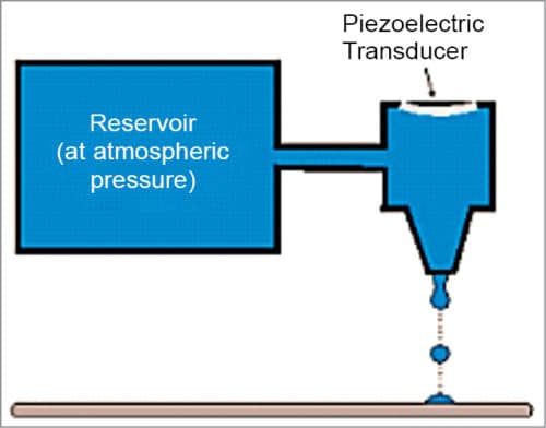
C60N as a dipole additive may be mixed, which increases power conversion efficiency due to more efficient extraction of photogenerated charge carriers. An ink made from a mix of polymer and fullerene derivative is used for ink-jet printing. Ink is then printed on a flexible substrate in 0.2-micrometre thickness to absorb Sun’s energy (Fig. 2). Using this incredible thin layering, one kilogram of polymer can be used to print a solar cell, the size of a football field.
Physics behind organic solar cells
A typical OPV device consists of a photoactive layer sandwiched between two electrodes, one of which has to be transparent to allow incoming light to reach the photoactive layer. Absorption of light excites the electron into the lowest-unoccupied molecular orbital (LUMO) of absorber material, creating strongly-bound electron-hole pairs called excitons.
Excitons must overcome their binding energy to dissociate. In the absence of a mechanism to dissociate excitons, these will spontaneously decay. In an organic bilayer device employing, say, copper phthalocyanine (CuPc)/perylene derivative, difference in electronic affinities between these two materials creates an energy offset at their interface, driving exciton dissociation.
Similar to this early device, many OPVs now have an active layer consisting of two materials, one electron donor that is a conjugated material and the other electron acceptor, which is a fullerene derivative.
Conjugated polymers are a particularly interesting class of organic semiconductors, as polymer conductivity can be easily and reversibly varied by doping, resulting in a range in conductivity from insulating to metallic. PEDOT, acronym of poly (3, 4-ethylenedioxythiophene), P3HT: poly (3-hexylthiophene), PANI (polyaniline), etc are conjugated polymers.
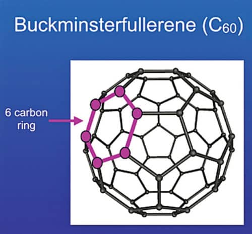
A fullerene is an allotrope of carbon whose molecules consist of carbon atoms connected by single and double bonds to form a closed or partially-closed mesh. The molecules may have various shapes like sphere, ellipsoid, tube, etc. These are denoted by their empirical formula written as Cn, where n is the number of carbon atoms. A model of C60 fullerene is shown in Fig. 3.
Once excitons are generated in the absorber material, they need to reach the donor-acceptor interface to be dissociated. Lifetime of excitons is finite and so is their diffusion length, which is around ten nanometres in conjugated molecules. If the donor-acceptor interface is too far from the point where excitons are generated, excitons will decay before reaching the interface and will not yield free charge carriers.
Diffusion of excitons is a severe limit for the performance of donor-acceptor bi-layer. On one hand, thickness of the photoactive layer has to be around hundred nanometres to efficiently absorb light; on the other hand, in a hundred-nanometres-thick bi-layer, only a small fraction of excitons would be generated close enough to the donor-acceptor interface.
One solution to solve this problem is to construct the active layer as BHJ instead of bi-layer, as shown in Fig. 4. Architecture of the BHJ solar cell was invented in 1995. BHJ concept involves self-assembly of nano-scale heterojunctions by spontaneous phase separation of donor and acceptor materials.
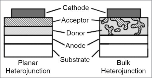
As a result of self-assembly, charge-separating heterojunctions are formed throughout the bulk of the material. Excitons that diffuse to the donor-acceptor interface can dissociate into free electrons and holes. Connecting the device to an external circuit, free charge carriers are then transported to contacts and extracted from the device, thus generating an electric current.
Negative and positive charges are present in the photovoltaic layer at the same time, thus there is a certain probability of recombination of charges. Recombination represents a loss process for a photovoltaic device because it reduces the number of charge carriers that contribute to photocurrent.
There are three fundamental processes that govern the operation of an OPV device, that is, generation, transportation and recombination of charge carriers, as shown in Fig. 5.
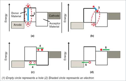
- Absorption of light generates an exciton marked as 1, which eventually diffuses towards donor-acceptor interface.
- Excitons are dissociated via charge-transfer, and a bound electron-hole pair (charge transfer state) may be formed.
- A further dissociation yields free charge carriers.
- Carriers are transported to electrodes.
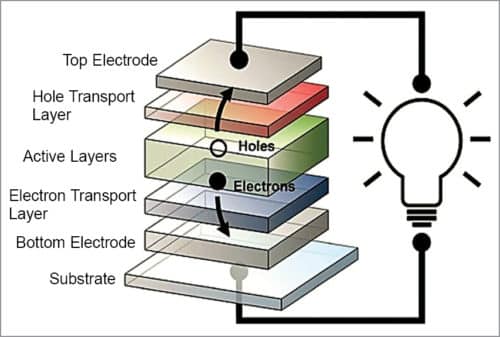
Organic solar cell structure and operation
As shown in Fig. 6, when sunlight strikes an organic solar cell, electrons in organic active layers pick up energy and begin moving through the core, leaving behind vacancies, called holes, which essentially move in the opposite direction. Electrons come out of the cell via one electrode, flow along an external circuit, powering a device along the way, and re-enter the solar cell through the second electrode, re-joining the holes they left behind. An electron transport layer and a hole transport layer facilitate the movement of electrons towards one electrode, and holes towards the other, thereby expediting one-way flow of current.
Over the past decade, researchers have made significant advances towards developing transparent organic solar cells, but they have encountered one persistent stumbling block—finding suitable materials for electrodes that carry current out of the cells. It is rare to find materials in nature that are both electrically-conductive and optically-transparent.
The most widely-used option is indium-tin-oxide (ITO). ITO is conductive and transparent but is also stiff and brittle. So, when the organic solar cell bends, ITO electrodes tend to crack and lift off.
However, indium is expensive and relatively rare. A promising alternative is graphene, a form of carbon that occurs in one-atom-thick sheets and has remarkable characteristics. It is highly-conductive, flexible, robust, transparent and inexpensive. A graphene electrode can be just one nanometre thick—a fraction as thick as an ITO electrode and a far better match for OPV.
Two key problems have slowed the wholesale adoption of graphene electrodes. The first is depositing graphene electrodes onto the solar cell. Depositing graphene as a top electrode onto the surface of hole transport layer (HTL) is tricky because HTL materials used during deposition process of graphene are soluble in water and sensitive to heat. Any error in the deposition process could destroy HTL materials.
The second problem is that the two electrodes need to play different roles. The ease with which a given material lets go of electrons is a set property called work function. In solar cells, just one of the electrodes should let electrons flow out easily. As a result, having electrodes made of graphene would require changing the work function of one of them so that electrons would know which way to go. But changing the work function of any material is not straightforward.
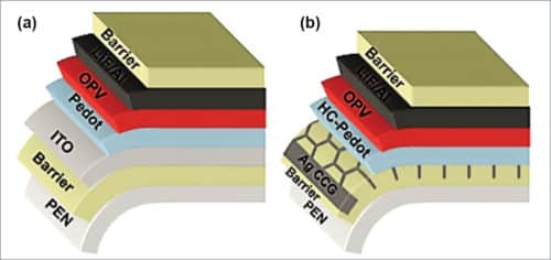
ITO-free TOPV
Use of a transparent conductive electrode such as ITO limits the reliability and cost of OPV devices, as it is brittle and expensive. Moreover, high sheet resistance of an ITO electrode on flexible substrates limits the maximum width of a single cell. Recent research work has developed an excellent alternative route incorporating ITO-free transparent anode having about 77 per cent transparency based on solution-processed, highly-conductive PEDOT:PSS in combination with a printed current-collecting grid made of ultra-thin silver metal. When a metal film is only a few nanometres thick, it becomes transparent. Schematic arrangement of an ITO-based/ITO-free device is shown in Fig. 7.
In an ITO-free device, highly conductive polymeric material, which is hundred nanometres thick, like, highly-conductive PEDOT:PSS, is used as a replacement for ITO. However, TOPVs with only PEDOT:PSS electrode do not provide high efficiency for large area devices due to limited conductivity of PEDOT:PSS.
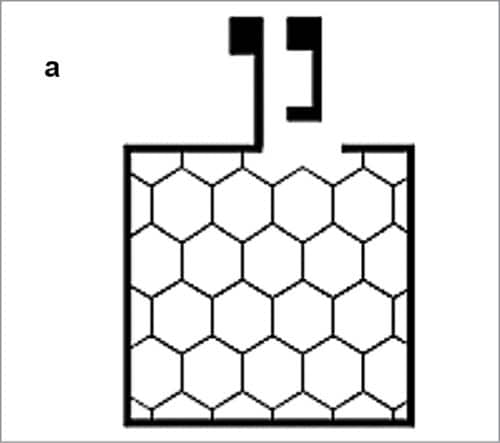
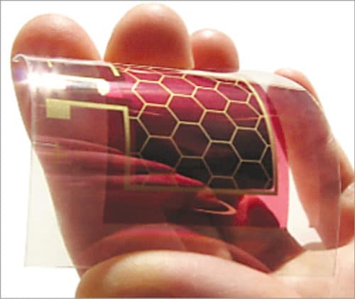
Improving conductivity of such a polymeric electrode is possible by combining it with a honeycomb-shaped silver metal grid patterned by suitably printing in a roll-to-roll processed device (Fig. 8). The printed silver metal grid shows a typical low resistance of one ohm per square. The grid is embedded in a barrier layer—a transparent polymer-based film.
Reactive materials used in OPV are sensitive to water vapour and other chemicals. To avoid deterioration, active material needs to be well-protected from water vapour and other chemicals by using barrier polymer base films. For manufacturing this device, HC PEDOT:PSS is dissolved in an organic solvent and a hundred nanometre-thick film is then deposited on the device by spin coating at 800rpm.
This type of compound anode has a sheet resistance (typically, fifteen-ohm per square) much lower than ITO anode. This is a cost-effective method of producing high-quality devices as the anode is fabricated from solution processing—no litho steps and no high temperature annealing are required.
Metal cathode (LiF/100nm thick Al) is made by thermal evaporation in a vacuum chamber through a shadow mask. It enhances electron injection, reduces interfacial resistance and prevents quenching of excitons. A transparent polythelene-naphthalate (PEN) film (hundred millimetres thick) is used as substrate, as it is strong, good insulator, has better heat transfer properties, and is moisture- and solvent-resistant. Anti-reflection coating is used on the outside surface to reduce reflection, because any light that reflects—potentially as much as ten per cent of the total—does not go through the device. The finished ITO-free device is shown in Fig. 9.
Rathindra Nath Biswas is a 1964-batch chemical engineering graduate from Jadavpur University, Calcutta. He was awarded a certificate for designing Benzol Plant by Giprokoks, USSR, and Certificate of Honour by Indian Institute of Metals. He has published 35 research papers in various journals. He retired from service as head – MECON, Durgapur.