Introduction
Electromagnetic Interference (EMI) compliance testing naturally comes at the end of a product development cycle. Not passing EMI is the system engineer’s worst fear. It means a major setback to the product shipping schedule and could also mean a costly total power re-design. Fortunately, designing a power solution that is EMI compliant doesn’t have to be a hit or miss effort. A well-planned design using a proper filter, low EMI components, low EMI power regulator ICs, and/or low EMI power modules, along with good PCB layout and shielding techniques, will assure a high chance of first-pass success.
What is EMI Noise? Why Should You Care?
EMI is the disruption of operation of an electronic device when it is either connected to, sharing the same power source with, or near another electronic device that generates the EMI. EMI can be either conducted or radiated. EMI problems can prevent adjacent pieces of electronics equipment from working alongside one another.

Common examples of EMI in our everyday life that you may have encountered are:
- Disturbance in the audio/video signals on the radio or TV due to an aircraft flying at a low altitude
- Transmitters that prevent local TV stations from displaying their pictures. In the worst case, the whole picture could disappear, or there may be some patterning of the picture.
- Interference caused by a cell phone’s handshake with the communication tower to process a call (this is why airliners ask passengers to switch off their cell phones during flights)
- Interference from a microwave oven that affects the nearby WiFi signal
With the vast growth in the usage of electronic equipment, the issue of electromagnetic compatibility (EMC) has become an important topic. Hence, standards bodies have been established to ensure proper performance of electronic equipment even with EMI. Now, with modern electronic equipment, it is possible to operate mobile phones and other wireless devices near almost any electronics equipment with little or no effect. This has come about by ensuring that equipment does not radiate unwanted emissions, and also by making equipment less vulnerable to radio frequency radiation.
EMI Design Requirements
The CISPR 22 (often referred to as EN55022 in Europe) EMI specification divides equipment, devices, and apparatus into two classes:

Class B: Equipment, device, and apparatus that are intended to be used in the domestic environment and meet CISPR22 Class B emission requirements
Class A: Equipment, device, and apparatus that do not meet the CISPR22 Class B emission requirements, but comply with the less stringent CISPR22 Class A emission requirements. Class A equipment shall have the following warning: “This is a Class A product. In a domestic environment this product may cause radio interference in which case the user may be required to take adequate measures.”
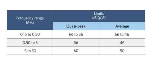
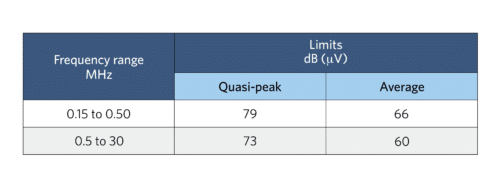
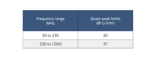
EMI testing comprises two parts: conducted and radiated. Conducted emission testing is done in the frequency range of 150kHz-30MHz. This is the AC current conducted into the line source and is measured using two methods: quasi-peak and average, each with their own limits. Radiated emission testing is done in the higher radio frequency range of 30MHz-1GHz. This is the radiated magnetic field from the device under test (DUT). The testing upper range, 1GHz, applies to the DUT that has an internal oscillator frequency up to 108MHz. This upper range extends to 2GHz with an internal oscillator up to 500MHz, 5GHz with an internal oscillator up to 1GHz, and 6GHz with an internal oscillator higher than 1GHz.
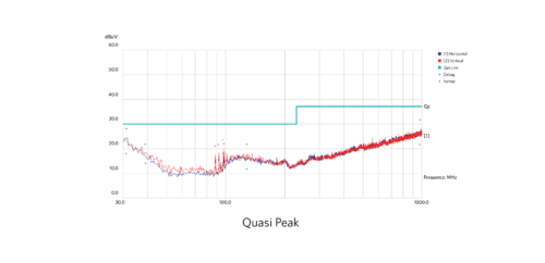
Below are graphical illustrations of the CISPR 22 specification: The y-axis is the EMI magnitude measured in dBuV. The x-axis is the frequency measured in Hz.
EMI Noise Sources in Switching Power Supplies
Switching power supplies can generate electromagnetic energy and noise as well as be impacted by electromagnetic noise from external aggressors. Noise generated by a switching power supply can be categorized as both conduction and radiation. Conducted emissions can take the form of voltage or current, and each of these can be further categorized as common-mode or differential-mode. Also, the finite impedance of connecting wires enables voltage conduction to cause current conduction and vice versa, and differential-mode conduction to cause common-mode conduction and vice versa.
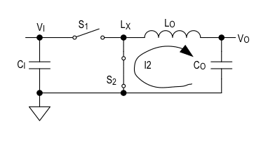
Let’s examine the noise sources in a switching power supply. Here is a simplified buck regulator schematic and its operational circuit waveforms:

Conducted EMI
As shown in Figure 5, the input current, II, of the buck regulator is a pulsing waveform, which is the main source of conducted, differential EMI injecting back into the power source VS. Conducted emissions are primarily driven by fast-changing current shapes at the input of the converter (di/dt). The value of conducted emissions is measured as voltage at the input of the converter, VS, using line impedance stabilization network (LISN). The input capacitor CI function is to filter out the AC (pulsing) component. The net current IS is the difference between II and ICI. We want IS to be DC or as smooth as possible. If CI is an ideal capacitor with infinite capacitance, it would keep VI constant and effectively filter out all AC component of I1, leaving a constant (DC) current flowing from the source VS and a constant DC voltage drop across the source impedance RS. In this case, the conducted EMI would be zero since IS is a DC current. In practice, we use a π-filter between the input source and the converter to contain conducted EMI within the regulatory limit.
Conducted emission usually poses a greater problem for fixed systems than for portable systems. Because the portable device operates from batteries, its load and source have no external connections for conducting emissions.
Radiated EMI
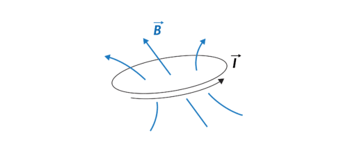
Radiated EMI are fast-changing magnetic fields that have high-frequency content of 30MHz and above. Magnetic fields are generated by the circuit’s current loops. Changing in these fields, if not properly filtered or shielded, can couple into other nearby circuitry and/or equipment and cause radiated EMI effects.
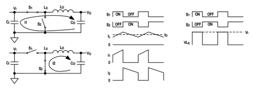
Figure 6 shows a buck converter with its fast di/dt current loops I1 and I2. The current loop I1 conducts during the on-time when S1 is on and S2 is off. The current loop I2 conducts during the off-time when S1 is off and S2 is on. The pulsating nature of the current loops I1 and I2 causes change in the magnetic fields with field strength propositional to the change of the current magnitude and the area of the conducting loop. Fast di/dt current edges generate high-frequency harmonics EMI in the regulatory radiated range. Keeping the area of these current loops small will minimize the field strength. Slowing down these edges will reduce the high-frequency harmonic content of the switching regulator, but slow transitions impact the regulator efficiency due to wasted energy. We’ll discuss ways to minimize the EMI radiation without impacting efficiency.
The voltage node LX (some vendors call it SW or other names) is a rectangular wave (ignore the parasitic ringing for now) that is connected to the inductor. Fast LX’s dv/dt voltage discontinuous edges couple high-frequency current to CO and the load through the output inductor’s parasitic capacitance, which can in turn generate EMI noise. It is important to minimize the output inductor’s parasitic capacitance to reduce this noise-coupling issue. LX also has high-frequency parasitic ringing. Using an RC snubber network from LX to GND helps reduce this ringing.
The same principle of the EMI noise sources described above applies to other switching-converter topologies as well. But the severity of the noise depends on the current and voltage wave shapes of a specific topology. For example, a boost converter running in continuous conduction mode has less conducted EMI component at its input, since its input current is more continuous compared to that of a buck converter.
Fixing EMI on a power system after the fact is hard, time consuming, and costly. Designing and planning for EMI compliance upfront is critical for project success. Common techniques to minimize EMI are line filtering, power-supply design, proper PCB layout, and shielding.
EMI Line Filtering Design
To reduce conducted emissions from a power converter, a π-filter is used between the input source and power converter. The design procedure to select the filter components is as follows:
1. Determine the input impedance RIN: The worst case closed loop input impedance of a buck converter is RIN = RO/D2 for all frequency where RO is the output load and D is the operating duty cycle. The minimum input impedance occurs when the converter is operating at minimum input supply voltage.
Example: Consider one of Maxim’s Himalaya SiP power modules, MAXM17575, a 4.5-60Vin, 0.9-54Vout that supplies up to 1.5A. Using MAXM17575 EV Kit as an example, the minimum input voltage is 7.5V. The output load is RO = Vo/Io = 5V/1.5A = 3.3Ω. The maximum operating duty cycle is D = VO/VINmin = 5V/7.5V = 0.66. So, the least possible input impedance is RIN = RO/D2 = 3.3 Ω /0.662 = 7.6Ω.2. Design the EMI filter with output impedance <= 10db lower than RIN: The addition of the input filter can affect the DC-DC converter’s performance. To minimize the effect, the output impedance of the filter must always be less than the input impedance of the power converter, for all frequency up to the converter’s crossover frequency.
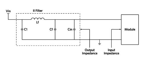
The output impedance of the LC filter at its resonance frequency, which is the highest value, is:
Zo=√(Lf/(Cf+Cin)
In our design we have considered the effective impedance of the filter to be 10dB less than the input impedance of the buck converter, which is approximately equal to one-third of the input impedance. For the MAXM17575 example, the required Zo is < =RIN/3 = 7.6/3 = 2.5Ω for all frequencies up to the MAXM17575 circuit’s crossover frequency, which is 45kHz.
PCB Layout Best Practices
PCB layout plays a significant role in EMI compliance success. A bad PCB layout can ruin a power converter with perfect electrical design. The following are good PCB layout practices to minimize EMI noise sources using the same buck converter example:
1. Minimizing high di/dt current loops: Properly place LO, CO, and S2 close together to minimize the I2 current loop. Then, place this entire group of components close to S1 and C1 to also minimize I1 current loop. When using a buck regulator IC (i.e. a buck controller with integrated power switches S1, and S2), it’s important to choose those ICs that have good pinouts to allow this minimization. The same consideration applies to using power modules.
2. Using Faraday shield: A Faraday shield (or cage), named after the English scientist Michael Faraday, is an enclosure used to block electromagnetic fields. There are two common ways to implement a Faraday shield in a power system:
a. A cage made of conductive material (such as copper) that encloses the entire power system or equipment. The electromagnetic field is contained inside the cage. This method is usually expensive due to the material cost of the cage and additional assembly labor.
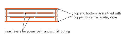
b. A layout with shielding ground planes on both the top and bottom of the PCB with a via connecting them to mimic a Faraday cage. All high di/dt loops are placed in the inner layers of the PCB so that our Faraday cage will shield the magnetic field from radiating outward. This method is lower cost and usually adequate to contain EMI. Figure 10 illustrates this technique.
Employing these PCB layout best practices provides a reasonable way to achieve EMI regulatory compliance without compromising power converter efficiency by otherwise slowing down the switching edges.
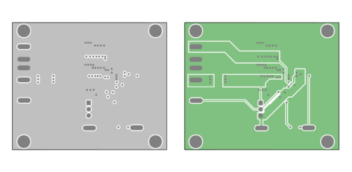
Now let’s consider Maxim’s Himalaya wide input IC, MAX17502, which operates at 4.5-60Vin, 0.9-54Vout supplying 1A current. The following is the MAX17502 EMI EVKIT PCB layout, using the Faraday shield technique (b). Figure 11a shows the top and bottom layers used as the Faraday shield. Figure 11b shows the second and third inner layers for routing. The second layer is used here as an extra shield, but it can also be used to route traces. In this layout, the high di/dt current loops I1 and I2 are routed on the third layer, which is completely enclosed in our Faraday shield.

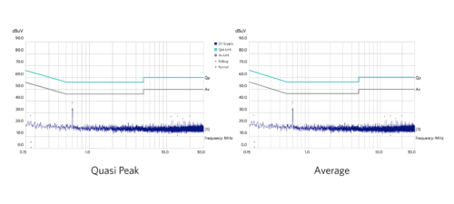
The following is the EMI test result of this MAX17502 EMI EVKIT, which passes CISPR 22 Class B with good margin.
Low EMI Power Components
Magnetic field from the output inductor can also radiate and cause EMI issues. Using a low EMI inductor reduces radiated EMI. Shielded inductors are recommended. This type of inductor has the magnetic field shielded and contained within the inductor structure. Avoid inductor types where the magnetic energy can radiate freely. Power modules using shielded inductors and employing good PCB layout practices will exhibit good EMI performance.
Low EMI Power Regulators and Modules
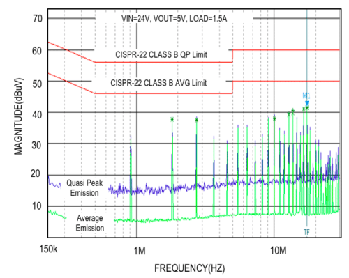
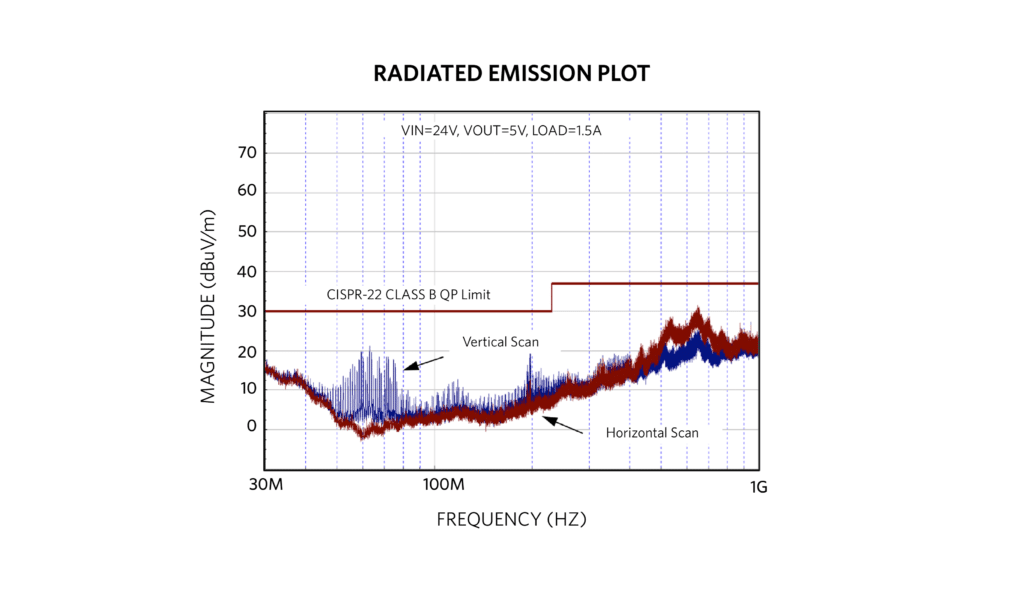
Maxim’s Himalaya regulator and power module families employ low EMI power inductors and good PCB layout practices, providing inherently low EMI power solutions. Using the Himalaya solutions means you don’t need to worry about compliance, unlike with other simplistic switchers in the market. Maxim has done all the work with the ICs, modules, and example reference layouts so that you can pass CISPR 22 (EN 55022) at optimal cost. The following are EMI test results of an example, MAXM17575, together with input EMI filter information:
|
Test Article (EUT)
|
MAXM17575
|
Result | PASS-EN55022 (CISPR 22) CLASS B |
| EUT Revision | REV-P1 | ||
| Input Voltage | 24V-Positive | Output Voltage | 5.0V |
| Switching Frequency | 900KHz | Output Current | 1.5A |
EMI Filter Configuration – Conducted EMI test
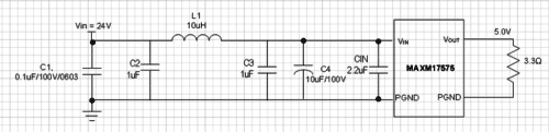
| Filter Component | Value | Part Number | Manufacturer |
| Inductor- L1 | 10uH | PA4332.103NLT | Pulse Electronics |
| Capacitor- C1 | 0.1uF | GRM188R72A104KA35 | Murata |
| Capacitor- C2, C3 | 1uF | GRM32CR72A105KA35 | Murata |
| Capacitor-C4 | 10uF | EEE-TG2A100P | Panasonic |
| Capacitor- CIN | 2.2uF | GRM32ER72A225KA35 | Murata |
EMI Filter Configuration – Radiated EMI test
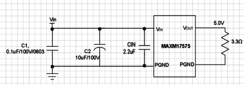
MAXM17575 has inherently very low radiated EMI. The input filter shown for the conducted EMI test is not needed and is not used for the radiated test. Using the input filter will provide additional passing margin for the radiated test result.
| Filter Component | Value | Part Number | Manufacturer |
| Capacitor- C1 | 0.1uF | GRM188R72A104KA35 | Murata |
| Capacitor-C2 | 10uF | EEE-TG2A100P | Panasonic |
| Capacitor- CIN | 2.2uF | GRM32ER72A225KA35 | Murata |
Summary
Planning for EMI compliance of a system upfront is critical for project success. This paper discussed common techniques to minimize EMI. The paper also presented guidelines for line filtering design, good PCB layout, and shielding practices, along with practical examples. A well-planned design using a proper filter, low EMI PMICs, components, and/or power modules, along with good PCB layout techniques and shielding, will assure a high chance of first-pass success.