Post-silicon validation includes a number of activities such as validation of both functional and timing behaviour as well as non-functional requirements. Each validation has methodologies to mitigate these. This part introduces the concept of validation.
Validation includes different tasks such as functional correctness, adherence to power and performance constraints for target use-cases, tolerance for electrical noise margins, security assurance, robustness against physical stress or thermal glitches in the environment, and so on. Validation is acknowledged as a major bottleneck in system-on-chip (SoC) design methodology. It accounts for an estimated 70 per cent of overall time and resources spent on SoC design validation.
Post-silicon validation is a major bottleneck in SoC design methodology. It takes more than 50 per cent SoC overall design effort. Due to increasing SoC design complexity coupled with shrinking time-to-market constraints, it is not possible to detect all design flaws during pre-silicon validation. Validation is clearly a crucial and challenging problem as far as diversity of critical applications of computing devices in the new era is concerned, along with the complexity of the devices themselves.

Post-silicon validation makes use of a fabricated, pre-production silicon implementation of the target SoC design as the validation vehicle to run a variety of tests and software. The objective of post-silicon validation is to ensure that the silicon design works properly under actual operating conditions while executing real software, and identify and fix errors that may have been missed during pre-silicon validation.
Complexity of post-silicon validation arises from the physical nature of the validation target. It is much harder to control, observe and debug the execution of an actual silicon device than a computerised model. Post-silicon validation is also performed under a highly-aggressive schedule to ensure adherence to time-to-market requirements.
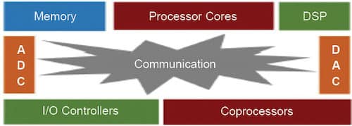
Post-silicon validation is done to capture escaped functional errors as well as electrical faults. Modern embedded computing devices are generally architected through an SoC design paradigm. An SoC architecture includes a number of pre-designed hardware blocks (potentially augmented with firmware and software) of well-defined functionality, often referred to as intellectual properties (IPs). These IPs communicate and coordinate with each other through a communication fabric or network-on-chip.
The idea of an SoC design is to quickly configure these pre-designed IPs for target use-cases of the device and connect these through standardised communication interfaces. This ensures rapid design turn-around time for new applications and market segments. It can include one or more processor cores, digital signal processors (DSPs), multiple coprocessors, controllers, analogue-to-digital converters (ADCs) and digital-to-analogue converters (DACs), all connected through a communication fabric.
Pre-simulation strengths show accurate logic behaviour—98 per cent of logic bugs found, 90 per cent of circuit bugs found, straightforward debugging and inexpensive bug fixing. Its limits are platform-level interactive and not real time.
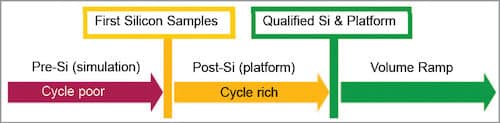
Post-simulation (platform) strengths show the actual target platform—two per cent of logic bugs found, ten per cent of circuit bugs found. Its limits are difficult debugging and expensive bug fix.
Focus areas of post-simulation are complementary to pre-simulation—exploiting post-simulation benefits (many cycles, platform-level interactions), ISA and features, memory sub-system/hierarchy, platform power state transitions, I/O concurrency, I/O margin characterisation and core circuit bug hunting.
Functional bug hunting
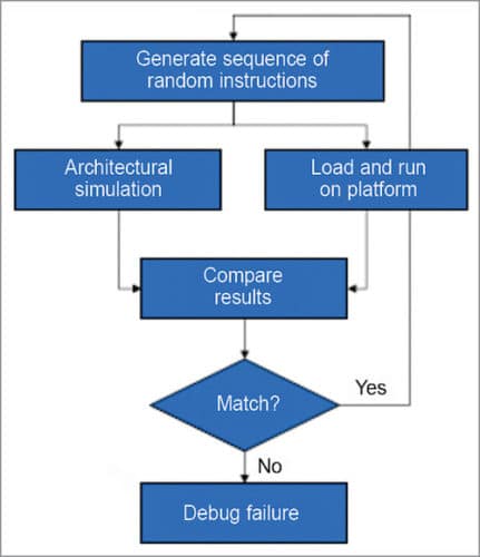
1. ISA architecture/micro-architecture testing is based on biased random schemes, such as random generation of instructions, checking based on architectural simulation, CPU core intensive, high throughput of random tests but typically low I/O stress and random power state transition injection.
2. Feature-oriented directed/random tests including paging, TLB and virtualisation.
Random instruction testing
1. Wide coverage of CPU/GPU cores
2. Strengths:
- Finds suble uarch bugs
- Stresses CPU pipeline boundary conditions
- Good at finding micro-code bugs
- High throughput core testing
3. Limits:
• Low I/O stress
• Need to complement with memory sub-systems tests
• Requires servers to generate instruction seeds
Memory sub-system validation
Options include:
1. Random and directed/random memory test strategy
2. Memory channel intensive
3. Based on multi-core and multi-processor configurations
4. When the target is standard and symmetric having multi-processor attributes like cache coherency, consistency and synchronisation, and memory ordering
I/O concurrency
1. The strategy here is to simultaneously load all platform buses.
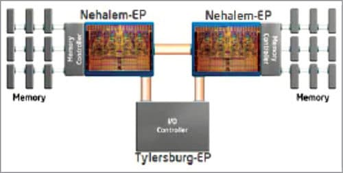
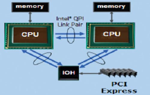
- Quick path interconnect
- DDR3 memory channels
- PCI Express Gen2
- USB, SSD
- SATA, PATA
- Display
2. Use of directed/random and biased random test generators
3. Test cards used to provide determinism
Compatibility and standards
1. Industry-standard operating systems (OSes), applications and peripherals are used to verify:
- Platform and component behavioural correctness
- Legacy compatibility of OS, applications and peripherals
2. Test configuration models and end-users
- Mobile and desktop client systems
- Blade and enterprise-level server systems
- Fully-integrated platforms: CPU, chipsets, BIOS, OSes and applications
3. Highly-stressful configurations, hunting for both functional and performance bugs
How circuit bugs appear
Some of the ways bugs appear:
1. Circuit bugs appear as DPMs—not all die or behave the same way
2. Taxonomy (classification)
(a) Timing convergence bugs
- Circuit operates too slow (speedpath),
- Circuit operates too fast (minimum delay), or
- Circuit fails due to timing of multiple converging signals (race)
(b) Analogue bugs:
- Primarily in I/O buffers, PLLs and thermal sensors
- Silicon does not operate in accordance with predicted (simulated) circuit behaviour
3. Fundamentals for circuit bug hunting are as follows:
(a) Needs a sufficiently large population of devices
(b) Needs to vary environmental conditions
(c) Needs to stimulate stressful system behaviour
(d) Stimulus is generally functional; failures look just like functional failures
Circuit debug issues
The following need to be checked for debugging:
1. On-die signal integrity
- Cross-coupling induced noise
- Droop-event induced noise
2. Power delivery integrity
- High dynamic current events
- Clock gating
3. Clock domain crossing
4. Process, voltage and temperature
- Power state transitions
- Silicon process variation
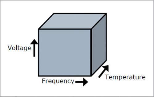
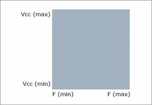
Ideal operating range
Ideally, silicon operates in well-defined volume. Minimum and maximum corners are defined as per manufacturers’ specifications: uniform over-voltage, frequency, temperature, process and time. But what happens is a bit different.
Other factors include temperature, component age and silicon variability.

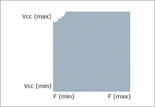
Speed paths
Circuit slows down as VCC decreases. And, failure disappears as VCC increases or F decreases. Historically, highest percentage of CPU circuit issues occur.
Minimum delays
Failure happens when circuit is too fast. Failure disappears as VCC decreases or F increases. This is hard to fix.
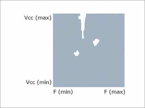
Shmoo holes/cracks
1. Voids within the window
2. Intermittent working
3. Multiple clock domains
- Skew within same domain
- Skew/jitter across domains
Finding circuit margins
1. Exercise in platform-based silicon characterisation
2. Method is stress-to-fail (increase FMAX to failure)
3. Stimulus is directed/random
- Victim/attacker patterns
- Software load-driven power variation
- Injected power state transitions
- Randomised instructions, memory configurations and architectural events
4. Characterised before/after burn-in (simulate aging)
5. Characterised over large populations to understand silicon variability
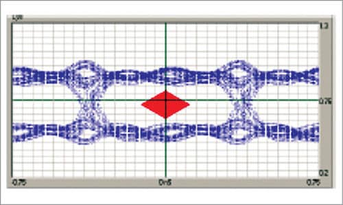
I/O margin characteristics
1. Stimulus includes victim/attacker patterns, resonance stimulus and other noise generators like dynamic CPU core loads
2. VCC and timing margined to fail (find extents of eye diagram)
3. Incorporates systematic 3D variation (shmooing) of voltage, temperature and frequency
4. Incorporates skewed silicon (varied process parameters) and skewed circuit boards (varied trace impedance)
Post-debug challenges
1. Basic observability is package pins
- Signal observability (higher integration SoC)
- Probing scope
- Probing signal integrity
2. Trend is towards lower observability. Integration increasing towards SoC
3. Functional and circuit issues require different solutions
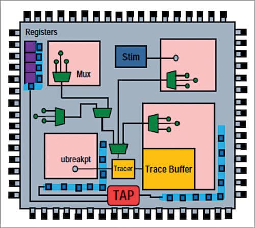
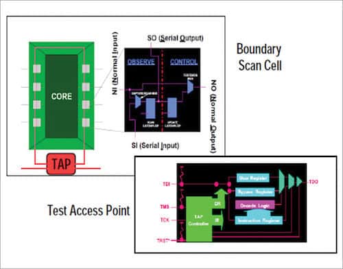
Observability/control/survivability architecture
Fictional example code:
// Read a counter in a certain design block on a certain boundary scan chain
// First select a desired design blockirscan(MY_CHAIN, SELECT_BLOCK_OPCODE)
// scan in block number stored in 4 bits.
drscan(MY_CHAIN , 4, BLOCK_NUMBER)
// now select the desired counter out of 100 counters
// 7 bits used to select counter
// This operation also resets counter to 0
irscan(MY_CHAIN, COUNTER_SELECT_OPCODE)
drscan(MY_CHAIN, 7, COUNTER_ID)
// Wait until something triggers…
// Read Counter Value
irscan(MY_CHAIN, READ_COUNTER_OPCODE)
drscan(MY_CHAIN, 32 , 0x0, Counter_Value)
Example of a boundary scan
Depending on the deployment target, use-cases and necessary power/performance trade-offs, any design functionality in an IP may be moved to hardware or software (firmware) implementation. Systems are vertically integrated with system use-cases only realised by hardware, software, applications and peripheral communication.
Validation and post-silicon validation is a complex co-validation problem across hardware, software and peripheral functionality, with no clear decomposition into individual components. With integration of significant design functionalities into one system, it is getting more and more complex to control and observe any individual design component as necessary for validation. And with reduced time-to-market, the number of silicon spins available for validation has decreased dramatically.
When an error is found in silicon, other errors are detected in the same silicon spin. In fact, tools, flows and design instrumentations have been incrementally accumulated over time in response to specific challenges or requirements. Over 20 per cent of the design real estate and a significant component of the CAD flow effort are devoted towards silicon validation today.
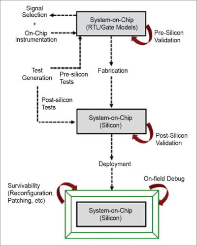
As we move from pre-silicon to post-silicon and finally on-field execution, more and more complex usage scenarios are exercised, potentially stimulating errors that could not be seen in previous validation phases. At the same time, observability and controllability of the design during these executions get progressively more complex, making it harder to root cause failure. At the same time, cost of a bug has increased and time available for debug decreased as we go further in the system lifecycle.
To be continued…
V.P. Sampath is a senior member of IEEE and a member of Institution of Engineers India, working in an FPGA design house. He has published international papers on VLSI and networks