Bringing a modern PCB design together into reality is often the real test. The third part of this series offers practical insights to streamline design, covering advanced PCB plating, manufacturing standards, compliance, and proven guidelines to prevent design oversights.
Outlining the step-by-step workflow, this part of the series dive deeper into the printed circuit board (PCB) plating process and explains how each stage strengthens circuit performance. By breaking the process into clear phases, this section highlights how effective plating directly contributes to reliable, consistent, and long-lasting electronic products.

Table of Contents
Advanced PCB plating process
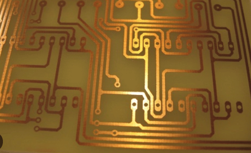
PCB plating is a key step in circuit board manufacturing. In this process, a thin metal layer is deposited on the PCB to improve electrical conductivity, strengthen connections, and protect the board from corrosion. This metallic layer ensures stable signal flow, enhances durability, and supports long-term performance. By reinforcing critical pathways and component interfaces, PCB plating helps electronic devices operate more reliably, efficiently, and safely throughout their lifespan.
- Surface preparation: The PCB is cleaned to remove contaminants using a combination of chemical treatments (etching, cleaning) and mechanical methods (scrubbing).
- Copper cladding: The board is coated with a thin layer of copper, which serves as the base for the subsequent plating.
- Activation: The surface is treated with an activating solution, which prepares the copper for the plating process by making it receptive to metal.
- Electroplating: A metal (typically copper, gold, or nickel) is deposited onto the PCB by an electrochemical process, where an electric current is passed through a solution containing metal ions, causing the metal to plate onto the PCB surface.
- Post-plating: The PCB is cleaned again and inspected for uniformity and defects in the plating.
This process enables durable, reliable electrical connections on the PCB.
The methods involved in plating
- Additive manufacturing: This process builds up circuitry by adding conductive material (typically copper) onto a bare epoxy laminate, adding material only where needed to form the desired traces.
- Subtractive manufacturing: This method is used for inner layers of the PCB, where a thin layer of copper is already on the board. Excess copper is removed using two methods:
- Computer-controlled machine (CNC) milling: This method is a dry process. The CNC machine will mill the copper and define traces and pads. It’s slow and mainly used for prototypes.
- Chemical method: This is Wet processing. It involves chemical methods for etching and removal of excess copper to form the final traces.
The choice of method depends on factors like the number of layers, trace current requirements, and design specifications.
Commonly used plating types
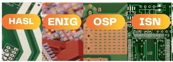
Immersion deposition:
In PCB manufacturing, two common immersion deposition processes are ENIG (Electroless Nickel/Immersion Gold) and Immersion Silver surface finishes, both used to protect solderable copper surfaces until assembly:
- ENIG: A more expensive and durable process where nickel is plated onto the PCB, followed by immersion gold. A key design consideration for ENIG use is the ‘solder mask’ to protect the conductive feature from moisture and oxidation. Without a solder mask, the catalyst could adhere directly to the laminate, allowing electroless metal to plate onto the catalyst, which may cause electrical issues. Manufacturers typically mitigate this risk, but using a solder mask is generally considered best practice in PCB design.
- Immersion silver: A cost-effective process where silver is applied to the PCB to protect the copper. There are no significant design considerations beyond standard design practices. The challenge with immersion silver is potential self-life degradation over time.
- Organic solderability preservative (OSP): OSP is a PCB surface finish. It is an organic coating, typically an azole-based compound, applied to the copper pads and traces of a printed circuit board. This coating prevents the copper from tarnishing or oxidising before soldering, allowing reliable connections.
- Hot air solder levelling (HASL): HASL is a common PCB surface finish that involves coating the exposed copper on a circuit board with solder. This process is achieved by immersing the board in molten solder and then using hot air to level the solder and remove excess material, thereby creating a protective, solderable surface.
PCB manufacturing standards and compliance
PCB manufacturing has evolved significantly over the past 50 years. In recent years, it has become a complex, multi-step process involving mechanical, chemical, and hybrid methods. There are some essential steps:
- Design and specifications: Before production begins, designers must carefully check their PCB designs and submit accurate specifications. This includes choosing the appropriate finish type, solder mask colour, and any special features. Inaccurate specifications can lead to confusion, delays, and extra costs. If using a computer-aided design (CAD) tool with a design for manufacturing (DFM) check, it is wise to run it to avoid production issues.
- CAM tooling: The design files are sent to the computer-aided manufacturing (CAM) department, where they’re reviewed for potential issues and converted into a format usable for manufacturing. The CAM team ensures the design is complete, conducts engineering reviews, and optimises for production efficiency.
- Transferring design to panel: The design is transferred onto a copper-clad panel using a photosensitive polymer and ultraviolet (UV) light. This step creates the initial traces, pads, and through-holes.
- Drilling and plating: Precision drilling machines are used to create small holes and vias, essential for connecting different PCB layers. Copper plating is then applied to these vias and external circuitry to provide electrical conductivity between layers.
- Etching: Excess copper is removed, revealing the final circuit in the layout. The PCB should now function electrically as designed.
- Solder mask and surface finish: A solder mask is applied to protect the board from oxidation and prevent solder bridging. A surface finish is then added to exposed copper to further protect against corrosion and to ensure a suitable environment for soldering during assembly.
- Legend and labelling: This is also called the silkscreen process. It adds labels, part reference markers, and designators to aid in component placement and orientation during assembly. The quality of silk screen legibility varies based on the type of silk printing method. For example, Injective printing and direct printing. Designers need to take care that the font size and spacing of the legend are maintained for better readability.
- Routing and final inspection: The PCB is separated from the manufacturing panel, and any cut-outs, slots, or non-plated holes are made. After routing, the board undergoes final inspection and is prepared for shipment.
Throughout the process, every mechanical and chemical step introduces potential variations. Designers must account for these by following best practices, using appropriate tolerances, and verifying manufacturability. As designs become increasingly complex (like smaller hole diameters, more layers, and lower-aspect-ratio vias), it is crucial to account for these variations to avoid manufacturing issues. Additionally, understanding industry standards, such as IPC-2615, and planning for worst-case scenarios during design will help ensure a robust final product.
Applying best practice guidelines in PCB design to avoid oversights
Designing a printed circuit board involves making numerous critical decisions. Key principles can simplify this process. When possible, use the largest formats for copper spacing, trace widths, and hole sizes to improve yields, reduce costs, and avoid production issues. Collaborate with your supplier to align design choices with manufacturing capabilities, maximising production efficiency. Stick to conventional design techniques unless necessary, as advanced features such as blind and buried vias can increase costs and complexity. Engage with assembly partners early to optimise layout for cost and reliability.
Designers should consider the following best practice guidelines to overcome:
1. Define design requirements clearly
- Understand functional needs: Understand the application and define the floor plan. Get the required design input of the electrical requirements before starting.
- Select appropriate materials: Choose the right PCB substrate (like FR-4, Rogers) based on signal speed, thermal requirements, and mechanical strength.
- Set design constraints: Specify layer count, trace width, impedance requirements, and spacing.
2. Follow good schematic design practices
- Organised schematics: Arrange the schematic logically to make connections clear.
- Label components clearly: Use descriptive and unique component labels as per IPC standards (R1, C2, U1, D1).
- Add annotations: Include notes for critical components or connections.
- Use simulation tools: Verify circuit behaviour before PCB layout.
3. Plan the board layout thoughtfully
- Component placement:
- Place critical components (microcontrollers, power supplies) first.
- Group components (place decoupling capacitors close to IC pins).
- Maintain symmetry and balance in placement to reduce mechanical stress.
- Signal path optimisation: Choose short, direct paths for critical signals, such as high-speed signals (like memories).
- Design for manufacturability (DFM): ensure sufficient clearance and run DFM checks with any PCB supplier.
- Design for testing (DFT): Allocate sufficient space for test points and component-to-component spacing to ensure testability.
- Design for assembly (DFA): Allow sufficient space for component assembly and rework.
4. Ensure robust power and ground design
- Dedicated power planes: Use separate planes for power and ground to reduce noise.
- Minimise ground loops: Choose a single-point ground reference where possible.
- Adequate decoupling:
- Place decoupling capacitors near IC power pins.
- Use capacitors of varying values to handle a range of frequencies.
- Wide traces for power: Use wider traces for power distribution to reduce resistance and heat.
5. Thermal management
- Thermal reliefs: Use thermal reliefs for pads connected to large copper areas.
- Heat sinks and vias: Add vias near heat-generating components to dissipate the heat.
- Consider airflow: Orient components to facilitate natural airflow.
6. Design for electromagnetic compatibility (EMC)
- Avoid antenna effects: Keep high-speed traces and loops small.
- Shielding: Use ground planes and shielding cans for EMI-sensitive circuits.
- Filter design: Add filters to suppress noise on power lines.
7. Mechanical and assembly considerations
- Board shape: Avoid sharp edges; round corners reduce stress.
- Component heights: Ensure tall components do not interfere with enclosures.
- Mounting holes: Add sufficient mounting holes with grounding where needed.
8. Test points and debugging
- Add enough test points for critical signals and power rails.
- Use accessible pads for probes for automated test equipment, like a test Jig.
9. Perform thorough reviews and simulations
- Design rule check (DRC): Validate the design against manufacturing constraints.
- Signal integrity analysis: Use tools to check for reflections, overshoot, and other issues.
- Thermal analysis: Take care that the board can handle heat under operating conditions.
10. Communicate with the manufacturer
- Provide clear documentation, including Gerber files, assembly drawings, and BOM (Bill of Materials).
- Understand the manufacturer’s capabilities (like minimum trace width, spacing, and via sizes).
- Provide proper fabrication documents and call out the correct IPC class as required.
- Any special processes, such as filling, tenting, and special plating, should be clearly communicated in the drawing so the manufacturer does not miss them.
11. Post-design testing and validation
- Prototype testing: Assemble and test prototypes before mass production.
- Functional testing: Verify that the PCB meets electrical and mechanical specifications.
- Iterative improvements: Address issues found in testing and optimise for final production.
Authored By: Ronak Desai and Santhosh Rangasamy
The authors, Ronak Desai, works at Infineon as the System Hardware Application Director. With over 22 years of experience in the embedded industry, he specialises in the design and development of embedded products and set-top box applications. His expertise encompasses microprocessor/microcontroller/RF and Wi-Fi-based products.
Santhosh Rangasamy works at Infineon. He has over 15 years of experience in PCB layout designing and package design, PCB 3D layout simulation, DFM, DFA & DFT for PCB.