


 The most commonly used multimeters and oscilloscopes are sold with simple non-symmetrical (single-ended) probes. But often we need differential probes to measure and observe signals between non-grounded test points.
There are different types of differential probes available, but most of them are costly. Also, some of these get damaged easily. And repair of probes (when possible) can be very expensive. Here is a simple and low-cost solution for the differential probes.
Circuit and working
The circuit diagram of a high impedance differential probe for oscilloscopes and multimeters is shown in Fig. 1. The probe has a high input resistance of 10-mega-ohm.
It is built around two popular integrated circuits—IC1 and IC2. IC1 is a dual operational amplifier (op-amp), which can be TL072, TL082, TL062, or a similar one. It should have JFET inputs and low noise.
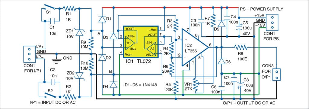
IC2 is a single op-amp such as LF356 and LF357. It should preferably have pins for offset control. IC2 can be TL071, TL061, TL081, etc. But the offset control should be changed.
The offset control is needed only in DC mode. IC1 and IC2 should have a low-temperature drift.
In order to keep the circuit as simple as possible, both inbuilt operational amplifiers in IC1 work as simple followers. The circuit has DC or AC inputs. If you close switches S1 and S2, the input of the probes is DC. If you open S1 and S2, the input of the probes is AC. Switches S1 and S2 should open and close simultaneously.
The inputs of IC1 are protected by resistors (R1 and R2), diodes (D1 through D4), and Zener diodes (ZD1 and ZD2). The differential voltage of the probe is limited by ZD1 and ZD2 at around 10V. The probe is intended to be used at much lower differential voltages. This is why the IC2 works like a differential amplifier with a gain of 10.
IC2 must have a gain product bandwidth (GBW) several times higher than the GBW of IC1. Or else, the IC2 will limit the bandwidth of the probe. If LF357 is used instead of LF356, the bandwidth will be greater.
In all the cases stated above, the 3dB bandwidth is above 30kHz. The power supply is at least 12V and preferably ±15V, and it should be well filtered. If LF356 or LF357 is used, the potmeter VR1 should be a multi-turn trimmer with a resistance between 22- and 27-kilo-ohm.
Construction and testing
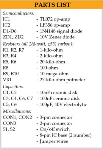
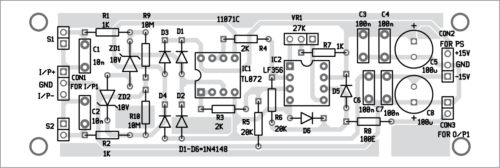
A PCB layout of a high impedance differential probe is shown in Fig. 2 and its components layout in Fig. 3. Assemble the circuit on the PCB. Connect ±15V power supply across CON2 on the PCB.

Download PCB and component layout PDFs: click here
Depending on the application, use an appropriate connector such as BNC at CON1.
Petre Tzv Petrov was a researcher and assistant professor at the Technical University of Sofia, Bulgaria and expert-lecturer in OFPPT (Casablanca), Kingdom of Morocco. Now, he is working as an electronics engineer in the private sector in Bulgaria.

Hello ,
This is an interesting project, but I’m starting to work with an oscilloscope. But I don’t get knowledge in this area yet…. Hence, I’ve a question, whether this probe will allow direct measurement of 230VAC voltage, without a necessary separation transformer for an oscilloscope.
I’m grateful for your reply.
Cheers , Irek